Review
. 2024 Sep 27;24(19):6264.
doi: 10.3390/s24196264.

Complementary Metal-Oxide-Semiconductor-Based Magnetic and Optical Sensors for Life Science Applications

Affiliations
Review

Complementary Metal-Oxide-Semiconductor-Based Magnetic and Optical Sensors for Life Science Applications

Tayebeh Azadmousavi et al. Sensors (Basel). .

Abstract

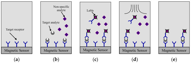
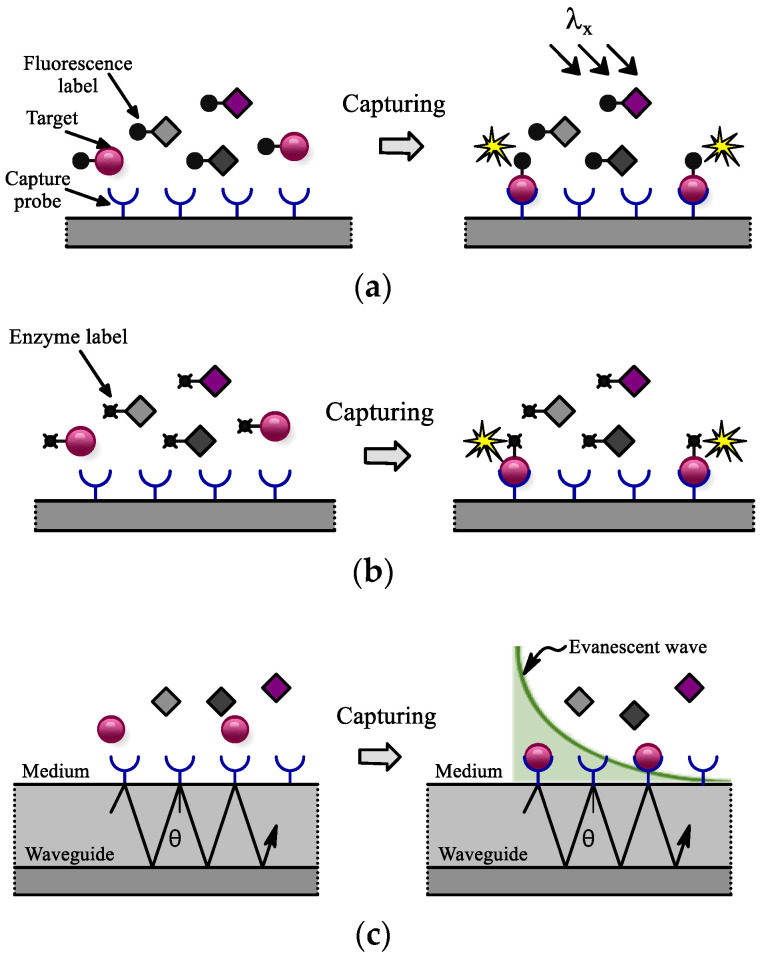
Optical and magnetic sensing methods are integral to both research and clinical applications in biological laboratories. The ongoing miniaturization of these sensors has paved the way for the development of point-of-care (PoC) diagnostics and handheld sensing devices, which are crucial for timely and efficient healthcare delivery. Among the various competing sensing and circuit technologies, CMOS (complementary metal-oxide-semiconductor) stands out due to its distinct cost-effectiveness, scalability, and high precision. By leveraging the inherent advantages of CMOS technology, recent developments in optical and magnetic biosensors have significantly advanced their application in life sciences, offering improved sensitivity, integration capabilities, and reduced power consumption. This paper provides a comprehensive review of recent advancements, focusing on innovations in CMOS-based optical and magnetic sensors and their transformative impact on biomedical research and diagnostics.

Keywords: CMOS; PoC diagnostic; magnetic sensors; optical sensors.


Conflict of interest statement

The authors declare no conflict of interest.

Figures

Figure 1
Figure 1
Illustration of a CMOS sensing platform consisting of a CMOS chip integrated with an electronic printed circuit board (PCB) for interfacing with a computer wirelessly. The data are transferred for AI cloud computation. The sensor can be magnetic, optical, or utilize other methods.
Figure 2
Figure 2
Magnetic sandwich immunoassay process: (a) the sensor surface is functionalized with a capture antibody, (b) the surface is then exposed to the sample, (c) a magnetically labeled detection antibody is introduced, (d) any non-specifically bound labels are washed away, (e) counting the remaining labels yields a measurement of the target concentration in the sample [17].
Figure 3
Figure 3
Differential magnetic sensing based on LC cross-coupled oscillator.
Figure 4
Figure 4
Cross section of a Hall effect sensor for magnetic bead detection [49].
Figure 5
Figure 5
Schematic overview of the measurement setup for detecting a single magnetic microbead with a silicon Hall effect sensor.
Figure 6
Figure 6
Post-processing etching steps conducted after CMOS fabrication aim to minimize the distance between the magnetic sensing region and the Hall sensors.
Figure 7
Figure 7
The block diagram of the array of Hall effect magnetic sensors based on magnetic relaxation [49].
Figure 8
Figure 8
(a) Illustrative diagram of the GMR SV sensor film stack and (b) the readout circuit.
Figure 9
Figure 9
The fundamental principle operation of the NMR system. (a) The core of the NMR system; (b) the switch is connected to the TX, and B1 is generated to excite the sample; (c) the switch is connected to the RX, and the spins are relaxed by the relaxation time of T2.
Figure 10
Figure 10
The structure of the NMR system consisted of an RF transceiver, a portable permanent magnet, and in-house fabricated 500 nH planar microcoils.
Figure 11
Figure 11
The architecture of spectrometer.
Figure 12
Figure 12
Optical detection principle. (a) Fluorescence, (b) bioluminescence, (c) evanescence wave.
Figure 13
Figure 13
Readout circuit of a fully integrated fluorescence-based sensor for dynamic monitoring of living cells.
Figure 14
Figure 14
Schematic of the pseudo-differential pixel.
Figure 15
Figure 15
Photocurrent readout for bioluminescence detection.
Figure 16
Figure 16
(a) Structure of an MRR and (b) Lorentzian spectrum of the ring.
Figure 17
Figure 17
(a) A photodetector and a TIA transform the optical signal into the electronic domain. (b) The neff causes a resonant shift in the ring, denoted as λres. When operating at a constant input wavelength, this resonant shift results in fluctuations in the POut.

References

    1. Syu Y.-C., Hsu W.-E., Lin C.-T. Field-effect transistor biosensing: Devices and clinical applications. ECS J. Solid State Sci. Technol. 2018;7:Q3196. doi: 10.1149/2.0291807jss. - DOI
    1. Sadighbayan D., Hasanzadeh M., Ghafar-Zadeh E. Biosensing based on field-effect transistors (FET): Recent progress and challenges. TrAC Trends Anal. Chem. 2020;133:116067. doi: 10.1016/j.trac.2020.116067. - DOI - PMC - PubMed
    1. Panahi A., Ghafar-Zadeh E. Emerging Field-Effect Transistor Biosensors for Life Science Applications. Bioengineering. 2023;10:793. doi: 10.3390/bioengineering10070793. - DOI - PMC - PubMed
    1. Ghafar-Zadeh E., Sawan M., Chodavarapu V.P., Hosseini-Nia T. Bacteria growth monitoring through a differential CMOS capacitive sensor. IEEE Trans. Biomed. Circuits Syst. 2010;4:232–238. doi: 10.1109/TBCAS.2010.2048430. - DOI - PubMed
    1. Couniot N., Francis L.A., Flandre D. A 16 × 16 CMOS capacitive biosensor array towards detection of single bacterial cell. IEEE Trans. Biomed. Circuits Syst. 2015;10:364–374. doi: 10.1109/TBCAS.2015.2416372. - DOI - PubMed

LinkOut - more resources