. 2024 Oct 18;14(1):24434.
doi: 10.1038/s41598-024-72634-2.

Micron-scale imaging using bulk ultrasonics

Affiliations

Micron-scale imaging using bulk ultrasonics

Loheshwaran Chandran et al. Sci Rep. .

Abstract

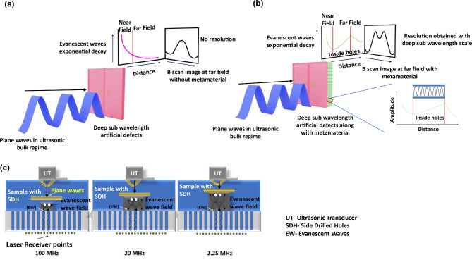
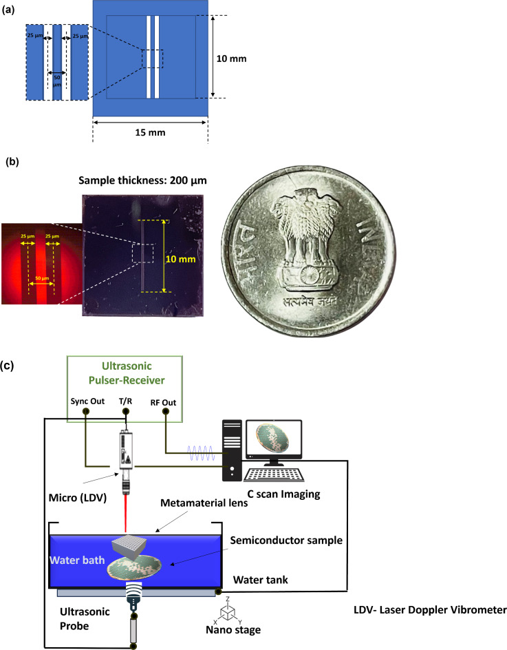
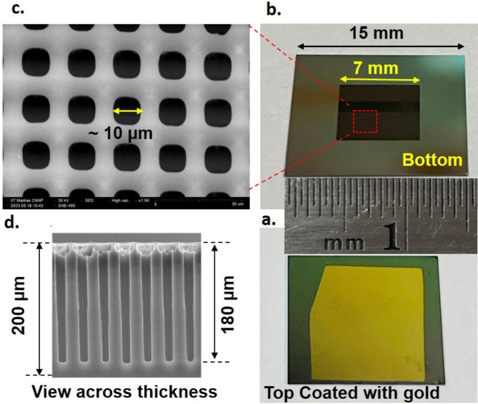
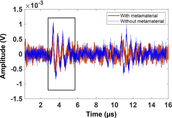
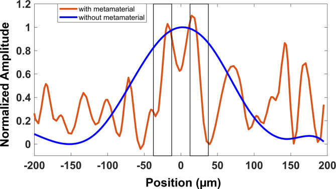
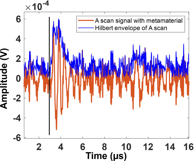
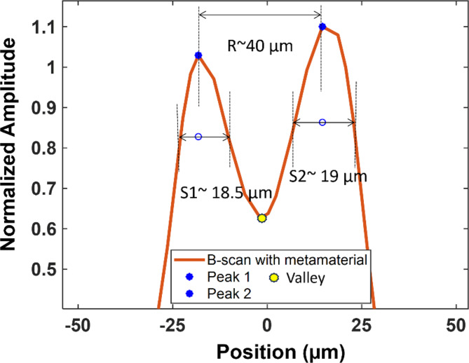
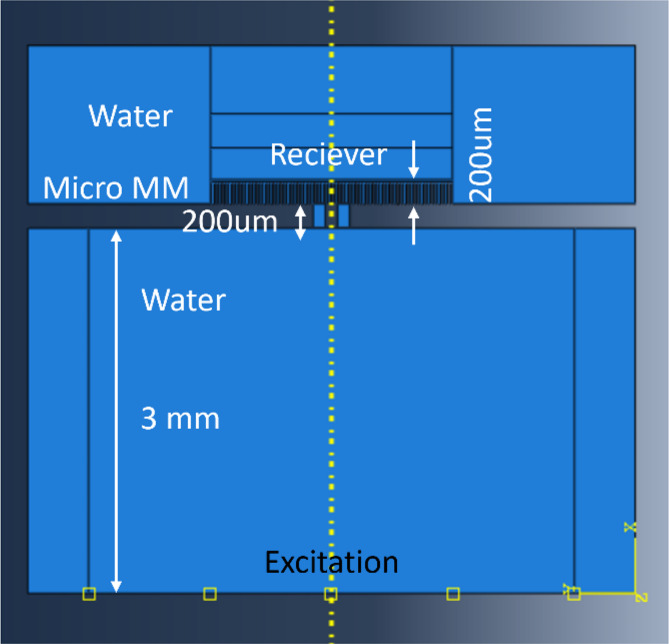
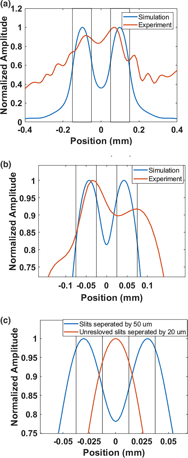
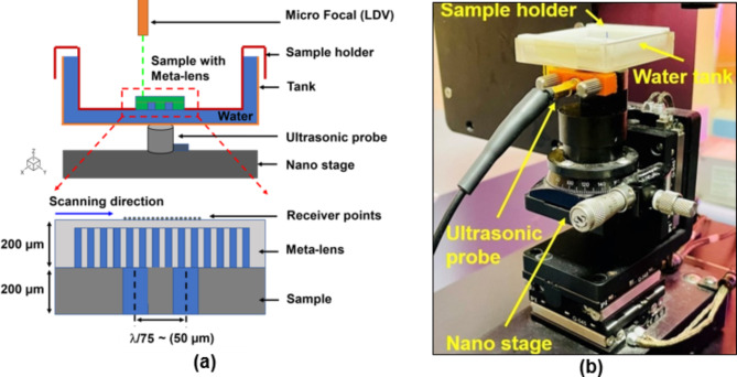
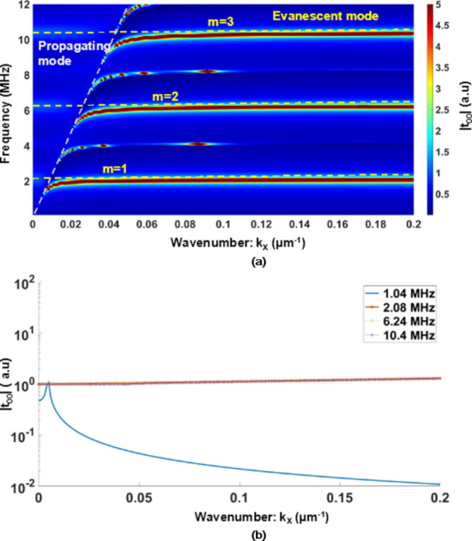
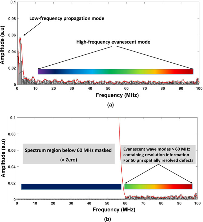
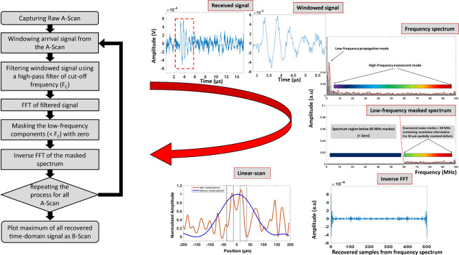
An extraordinary resolution down to 50 microns is demonstrated for the first time for bulk ultrasonics, using novel micro-fabricated metamaterial lenses. The development and performance of the silicon-based Fabry-Perot type metalenses with an array of 10 micrometre square holes are discussed. Challenges in wave reception are addressed by a custom-developed micro-focal laser with a sub-micron spot size and an innovative experimental set-up together with physics based signal processing. The results provide a pathway for material diagnostics at greater depths with high resolution using micro-metalens-enhanced ultrasound as an alternative to expensive and radiation prone electromagnetic techniques.

Keywords: Acoustic microscopy; Micro metamaterial; Periodic holey structures; Rayleigh diffraction limitation; Sub-wavelength imaging.


Conflict of interest statement

The authors declare no competing interests.

Figures

Fig. 1
Fig. 1
Schematic illustration of the utility of metamaterial: (a) Line scan obtained without metalens; (b) Line scan obtained with metalens (Inset represents Fabry Perot resonance); (c) The relationship between frequency and detectable region (evanescent wave field) within the material for commercially available probes of 100 MHz, 20 MHz, and 2.25 MHz (Arrows represent the direction of wave propagation).
Fig. 2
Fig. 2
Sample and defects studied in this paper: (a) Schematic of the slit-type defects created in a silicon wafer; (b) A photograph of the sample with defects considered for resolution demonstration (Inset is the snapshot of an optical microscopic image of the defects); (c) Schematic of the experimental setup developed by the authors for micron-scale defect characterization using linear bulk ultrasonics, as discussed in this paper.
Fig. 3
Fig. 3
Photographs of micro fabricated metalens: (a) Top coated with a thin layer of gold for high reflectivity for micro-focal ultrasonic laser reception and (b) Bottom view showing metamaterial mesh with scale; and SEM images of mesh (c) Viewed from the bottom; (d) Viewed from the side.
Fig. 4
Fig. 4
An example time trace or ‘A-scan’ from the experiment with and without microfabricated metalens (the first arrival of the received signal is windowed for further analysis).
Fig. 5
Fig. 5
‘B-scan’ results based on post processed ultrasonic data obtained from a linear scan experiment across the sample by the LDV in spatial steps of 10 μm, demonstrating a defect separation resolution down to 50 μm for the bulk ultrasonic regime achieved using the microfabricated metalens discussed in this paper (rectangular box denotes defect locations).
Fig. 6
Fig. 6
A-scan obtained in experiments with for the case metamaterial, shown together with a Hilbert envelope (dashed vertical line denotes the time of arrival of the wave packet of interest).
Fig. 7
Fig. 7
B scan obtained from experiments demonstrating 50 μm resolution (S1 and S2 are observed slit sizes).
Fig. 8
Fig. 8
Snapshot showing FE model considered for finding resolution limit.
Fig. 9
Fig. 9
Simulation and experimental plots of amplitude across B-scans showing resolution at resonant frequencies (a) Slits are separated by 200 μm; (b) Slits are separated by 100 μm; (c) Simulation plots of amplitude across B-scan showing resolution of slits separated by 50 μm and no resolution for the slit size of 20 μm (Rectangular box denotes the slit placement).
Fig. 10
Fig. 10
Through-transmission ultrasonic scanning of silicon sample with sub-wavelength defects by micro-focal LDV and micro-metalenses: (a) Schematic illustration (not to scale); (b) Photograph of actual experimental configuration.
Fig. 11
Fig. 11
Dispersion relation: (a) Modulus of transmission coefficient versus parallel momentum (x-axis) and frequency (y-axis). At the Fabry–Perot resonance modes (m = 1,2,3). The flatness of the dispersion curves can clearly be observed; (b) Modulus of zero-order transmission coefficient evaluated for 3 different frequencies; The first corresponds to the half of the 1st Fabry–Perot resonant frequency and the remaining three correspond to the three lowest Fabry–Perot resonant frequencies (m = 1,2,3).
Fig. 12
Fig. 12
Processed spectrums of an arbitrary A-scan taken from 50 μm spatially resolved:  (a) Without masking propagating modes; (b) With masking propagating modes.
Fig. 13
Fig. 13
Process flow for fabrication of micro-metalens (Note: dimensions are not to scale).
Fig. 14
Fig. 14
Illustration of water droplet contact angle measurements for 10 μm holes sample: (a) Before oxidation (contact angle > 90° indicates hydrophobic nature); (b) After oxidation (sample becomes hydrophilic and water enters inside micropores).
Fig. 15
Fig. 15
(a) Schematic layout of ultrasonic microscope detection system, provided by Intelligent Optical Systems. Red line represents fibre optic cables, while green line represents electrical cables; (b) Snapshot of microscopic image capture through inbuilt microscope, showing focal spot (yellow spot) of diameter < 1 μm; (c) Calculation of laser spot size using standard 20–80 knife edge width.
Fig. 16
Fig. 16
Schematic illustration of experimental setup for demonstrating micron-scale sub-wavelength imaging (Insert shows the photo of nano stage, sample, and probe which are explained in Fig. 10b).
Fig. 17
Fig. 17
Schematic illustrating the approach for post processing of the A-Scan signal captured for a metalens enhanced line scan of the silicon sample with defects.

References

    1. Jensen, J. A. Medical ultrasound imaging. Prog. Biophys. Mol. Biol.93(1–3), 153–165 (2007). - PubMed
    1. Derby, B., Briggs, G. A. D. & Wallach, E. R. Non-destructive testing and acoustic microscopy of diffusion bonds. J. Mater. Sci.18(8), 2345–2353 (1983).
    1. Pendry, J. B. Negative refraction makes a perfect lens. Phys. Rev. Lett.85(18), 3966 (2000). - PubMed
    1. Saini, A., Felice, M. V., Fan, Z. & Lane, C. J. Optimisation of the Half-Skip Total Focusing Method (HSTFM) parameters for sizing surface-breaking cracks. NDT & E Int.116(1), 102365 (2020).
    1. Miura, K., Nasu, H. & Yamamoto, S. Scanning acoustic microscopy for characterization of neoplastic and inflammatory lesions of lymph nodes. Sci. Rep.3(1), 1255 (2013). - PMC - PubMed

LinkOut - more resources