. 2024 Oct 19;15(1):9042.
doi: 10.1038/s41467-024-52750-3.

Unidirectional ray polaritons in twisted asymmetric stacks

Affiliations

Unidirectional ray polaritons in twisted asymmetric stacks

J Álvarez-Cuervo et al. Nat Commun. .

Abstract

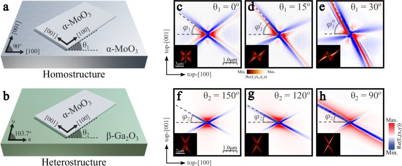
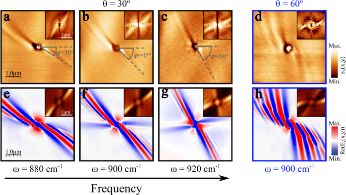
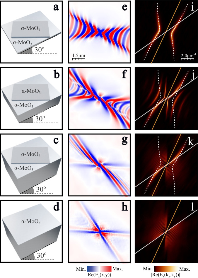
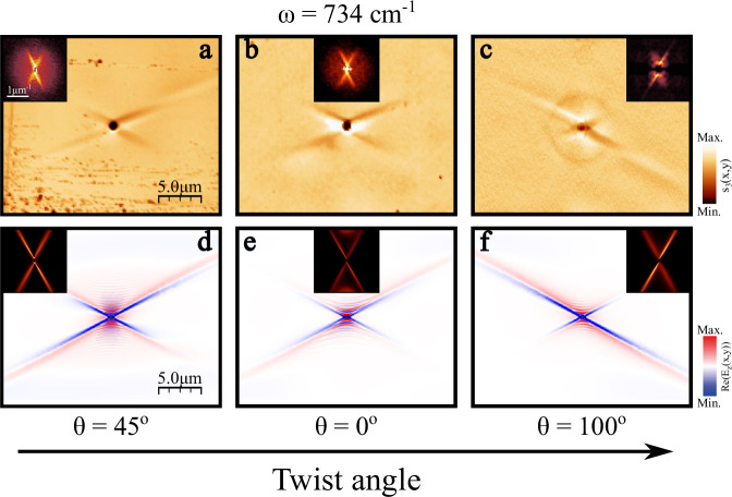
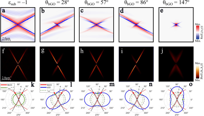
The vast repository of van der Waals (vdW) materials supporting polaritons offers numerous possibilities to tailor electromagnetic waves at the nanoscale. The development of twistoptics-the modulation of the optical properties by twisting stacks of vdW materials-enables directional propagation of phonon polaritons (PhPs) along a single spatial direction, known as canalization. Here we demonstrate a complementary type of directional propagation of polaritons by reporting the visualization of unidirectional ray polaritons (URPs). They arise naturally in twisted hyperbolic stacks with very different thicknesses of their constituents, demonstrated for homostructures of α -MoO3 and heterostructures of α -MoO3 and β -Ga2O3. Importantly, their ray-like propagation, characterized by large momenta and constant phase, is tunable by both the twist angle and the illumination frequency. Apart from their fundamental importance, our findings introduce twisted asymmetric stacks as efficient platforms for nanoscale directional polariton propagation, opening the door for applications in nanoimaging, (bio)-sensing, or polaritonic thermal management.


Conflict of interest statement

The authors declare no competing interests.

Figures

Fig. 1
Fig. 1. Unidirectional ray polaritons in twisted asymmetric stacks.
Schematic of the two systems under study: a a 80 nm-thin α-MoO3 layer placed over a 3 µm-thick α-MoO3 layer (homostructure) and b a 100 nm-thin α-MoO3 layer on top of a 5 µm-thick β-Ga2O3 layer (heterostructure). Parameters θ1 and θ2 represent the twist angle of the thick bottom layer with regard to the thin top layer for both systems, respectively. Real-space electric fields Re(Ez) launched by a point dipole source at the thin α-MoO3 surface for the homostructure (ce) and the heterostructure (fh) at illumination frequencies ω=920cm1 and 734 cm1, respectively. The twist angles are θ1=0o (c), 15o (d), 30o (e) and θ2=150o (f), 120o (g), 90o (h). The in-plane direction of ray-like propagation is marked with dashed gray lines at an angle defined by φ1,φ1, and φ1 (ce) and φ2 (fh) with respect to the [100] crystal direction of the top α-MoO3 layer. The Fourier Transforms (2D-FFTs) of the simulated real-space images are shown in the insets of ch. The same scale has been used for every simulated real-space map.
Fig. 2
Fig. 2. Observation of unidirectional ray polaritons in twisted asymmetric homostructures.
Near-field amplitude image in a twisted structure made of a 80-nm thin α-MoO3 layer over a 3-μm thick α-MoO3 layer with twist angles θ=30o (ac) and 60o (d) at an illuminating frequency of ω=880cm1, 900cm1, 920cm1 and 900cm1 for ad, respectively. A 200-nm diameter hole allows efficient launching of the phonon polaritons, whose wavefronts and direction of propagation are visualized by s-SNOM (scattering-type scanning near-field optical microscopy). For ac the in-plane direction of propagation is marked with gray lines at an angle defined by φ with respect to the [100] crystal direction of the top α-MoO3 layer, see Fig. 1a. The experimental isofrequency curves (Fast Fourier Transform (2D-FFT) of the near-field image) are shown in the insets, verifying polariton unidirectional propagation in the direction defined by φ. eh Simulated near-field amplitude images of the system in a (e), b (f), c (g) and d (h). The 2D-FFTs of the simulated images are shown in the top insets of eh.
Fig. 3
Fig. 3. Analysis of the thickness disparity in twisted homostructures.
ad Schemes of four systems made of α-MoO3 layers. The top thin layer in ac has a thickness of dtop=80 nm while the bottom has dbot=80 nm (a), dbot=500 nm (b), dbot=3 μm (c). Scheme d corresponds to a single thick layer of α-MoO3 (d= 3 μm). In all cases, the twist angle is θ=30o and the illumination frequency is ω=900cm1. eh Numerical simulations showing the near-field Re(Ez) generated by a point dipole located above the four structures represented in ad, respectively. il Isofrequency curves (IFCs) obtained by performing the Fourier Transforms (2D-FFTs) of the near-field images in eh, respectively. White dashed curves in ik correspond to the analytic IFC of the bilayer case shown in a. White and orange lines in il are the asymptotes of the IFCs of phonon polaritons in the bottom and top layers, respectively.
Fig. 4
Fig. 4. Observation of unidirectional ray polaritons in twisted asymmetric heterostructures.
Near-field amplitude image in a twisted heterostructure formed by a thin α-MoO3 layer with thicknesses dtop=200 nm (a, c) and 400 nm (b) on top of a 500-μm thick (010) β-Ga2O3 substrate with twist angles θ=45o (a), 0o (b), and 100o (c) at an illuminating frequency of ω=734cm1. A 1-μm diameter hole allows for the effective launching of the PhPs, whose propagation is visualized by s-SNOM (scattering-type scanning near-field optical microscopy). The experimental isofrequency curves, obtained by performing the Fourier Transforms (2D-FFT) of the near-field image, are shown in the insets. df Simulated near-field amplitude images of the system in a (d), b (e), and c (f). The 2D-FFTs of the simulated images are again shown in the insets. Both experimental and simulated images are aligned with the crystallographic axes of the top α-MoO3 layer.
Fig. 5
Fig. 5. Analysis of the ray asymmetry in twisted asymmetric heterostructures.
ae Simulated near-field amplitude images of a system made of a 100-nm thin α-MoO3 layer over an isotropic substrate with permittivity εsub=1 (a), and over a 5-μm thick β-Ga2O3 substrate with twist angles θ=28o (b), 57o (c), 86o (d) and 147o (e). The illumination frequency is ω=734cm1. fj Simulated isofrequency curves of ae obtained by performing the Fourier Transforms (2D-FFTs) of the simulated near-field images ae, respectively. ko. In-plane real permittivity values of α-MoO3 (red curve), an isotropic material with permittivity εsub=1 (green curve) and β-Ga2O3 (blue curve). The black straight lines represent the two angular directions of the α-MoO3 asymptotes which are defined by a zero-permittivity α-MoO3 value (red spots). The permittivity value of 1 for β-Ga2O3 is marked by a green spot. When the green and red spots are aligned, unidirectional ray-like propagation occurs along the corresponding asymptote. The black (green) dashed curve corresponds to the value ε=0 (ε=1) and is present for visual guidance.

References

    1. Basov, D. N. et al. Polaritons in van der Waals materials. Science354, aag1992 (2016). - PubMed
    1. Low, T. et al. Polaritons in layered two-dimensional materials. Nat. Mater.16, 182–194 (2017). - PubMed
    1. Caldwell, J. D. et al. Low-loss, infrared and terahertz nanophotonics using surface phonon polaritons. Nanophotonics4, 44–68 (2015).
    1. He, M. et al. Ultrahigh-resolution, label-free hyperlens imaging in the Mid-IR. Nano Lett.21, 7921–7928 (2021). - PubMed
    1. Autore, M. et al. Boron nitride nanoresonators for phonon-enhanced molecular vibrational spectroscopy at the strong coupling limit. Light Sci. Appl7, 17172 (2018). - PMC - PubMed

LinkOut - more resources