Review
. 2024 Oct 19;14(20):1679.
doi: 10.3390/nano14201679.

A Review of Wide Bandgap Semiconductors: Insights into SiC, IGZO, and Their Defect Characteristics

Affiliations
Review

A Review of Wide Bandgap Semiconductors: Insights into SiC, IGZO, and Their Defect Characteristics

Qiwei Shangguan et al. Nanomaterials (Basel). .

Abstract

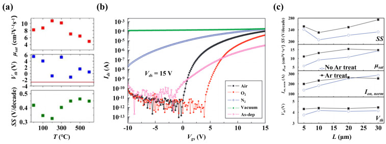
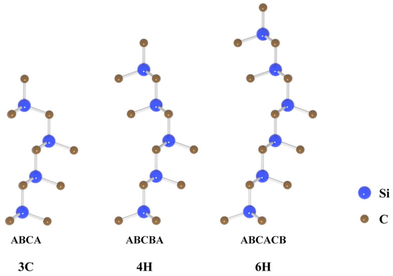
Although the irreplaceable position of silicon (Si) semiconductor materials in the field of information has become a consensus, new materials continue to be sought to expand the application range of semiconductor devices. Among them, research on wide bandgap semiconductors has already achieved preliminary success, and the relevant achievements have been applied in the fields of energy conversion, display, and storage. However, similar to the history of Si, the immature material grown and device manufacturing processes at the current stage seriously hinder the popularization of wide bandgap semiconductor-based applications, and one of the crucial issues behind this is the defect problem. Here, we take amorphous indium gallium zinc oxide (a-IGZO) and 4H silicon carbide (4H-SiC) as two representatives to discuss physical/mechanical properties, electrical performance, and stability from the perspective of defects. Relevant experimental and theoretical works on defect formation, evolution, and annihilation are summarized, and the impacts on carrier transport behaviors are highlighted. State-of-the-art applications using the two materials are also briefly reviewed. This review aims to assist researchers in elucidating the complex impacts of defects on electrical behaviors of wide bandgap semiconductors, enabling them to make judgments on potential defect issues that may arise in their own processes. It aims to contribute to the effort of using various post-treatment methods to control defect behaviors and achieve the desired material and device performance.

Keywords: 4H-SiC; a-IGZO; charge transition levels; defects; formation energy; post-process; stability.


Conflict of interest statement

The authors declare no conflicts of interest.

Figures

Figure 17
Figure 17
Schematic structures of typical SiC power devices, such as the (a) Junction-Barrier Schottky diode (modified structure of a Schottky barrier diode), (b) PiN diode, (c) planar-type vertical MOSFET, and (d) insulated gate bipolar transistor (IGBT). (e) Major application ranges in terms of the device blocking voltage for Si, SiC, GaN, and Ga2O3 power switching devices. (ae) Reprinted from [276], Copyright (2022) by The Japan Academy.
Figure 1
Figure 1
(a) and (b) Schematic illustrations of the InGaZnO4 in the crystal and amorphous phases. The amorphous phase is obtained by an MD-based melt-quench simulation using the crystal phase as the initio state. (c) Energy density curve calculated by DFT, where the diamond and star represent the energy of the individual configuration and the average energy at each density. (d) Schematic illustration of the real space overlaps among adjacent metal ns orbitals and oxygen 2p orbitals in AOS. The overlaps are crucial to maintain the electronic properties of AOS during the structure variation from crystal to amorphous state. (e) Energy band and (f) metal orbital DOS of an a-InGaZnO4 supercell containing 84 atoms generated by MD and calculated by GGA + U method. (c) Reprinted from [12], Copyright (2022) by John Wiley & Sons, Inc.
Figure 2
Figure 2
Ternary phase diagrams of IGZO fabricated by PEALD technology. The μFE, Vth (a), and Vth shifts under PBTS (b) are also shown. (a,b) Reprinted from [32], Copyright (2023) by Wiley-VCH GmbH.
Figure 3
Figure 3
Known subgap states in the band structure of a-IGZO. Reprinted from [6], Copyright (2019) by Wiley-VCH GmbH.
Figure 4
Figure 4
Local structure and formation energy of a-IGZO with VO. (a) Formation of Zn-Zn and In-Zn bonds. (b) Formation of In-In and Ga-Ga bonds. The VO is found to be located near Ga and Zn atoms, leading to the formation of huge voids. The In*-M bond is formed in the vicinity of the under-coordinated In (In*) by adding two electrons to the perfect a-IGZO. (c) Formation of the In*-M bonds and the intermediate normal state (NS) to transition state (TS). (d) Energy barrier diagram during the formation of the In*-M bond. (a) Reprinted from [38], Copyright (2018) by American Physical Society. (b) Reprinted from [41], Copyright (2010) by American Institute of Physics. (c,d) Reprinted from [42], Copyright (2014) by Nature Publishing Group.
Figure 5
Figure 5
(a) Schematic illustration of the orbital energy levels of a neutral O-O bond. The blue circles represent the pair of electrons donated by adjacent metal ions. (b) Local atomic configurations of the O-O bonds formed in a-InGaZnO4. These configurations include the disordered state (DS), transition state (TS), and peroxide state (PS) in the neutral condition, along with their corresponding +2 charged states DS*, TS*, and PS*. (c) Energy barriers associated with the formation and dissociation of the O-O bond calculated by DFT in both neutral (blue curve) and charged (red curve) states. (d) DOS for a-InGaZnO4 under different conditions. The O-O bond is formed by the introduction of Oi. (e) Band structure diagrams showing the instability caused by Oi under PBS. (ad) Reprinted from [38,49], Copyright (2015, 2018) by American Physical Society. (b,c) Reprinted from [50], Copyright (2012) by WILEY-VCH Verlag GmbH & Co. KGaA, Weinheim. (e) Reprinted from [51], Copyright (2017) by IEEE.
Figure 6
Figure 6
(a,b) Schematic diagram of the local a-IGZO structure with H impurities located at the VO positions and induced subgap states. Ht and Hd in (a) refer to H atoms that are triple-coordinated and double-coordinated. The blue arrow in (b) denotes the threshold photon energy (Eth, NBIS) associated with the NBIS phenomenon. (c) Schematic illustration of the integrated peak areas corresponding to the M-H and O-H vibrational modes in a-IGZO films, as determined by the TDS. (d) Diagram of H distributions in a-IGZO TFTs during PBTI and NBS. During PBTI, H+ are formed in HfO2 and moved to the channel, increasing carrier densities. Under NBS, H+ returns to HfO2 or changes to H in the channel. Both H states lead to negative ΔVth. (ac) Reprinted from [56], Copyright (2017) by AIP Publishing. (d) Reprinted from [63], Copyright (2024) by IEEE.
Figure 7
Figure 7
Stability issue of a-IGZO TFTs. (a) Vth recovery process in dark and light environments. (b,c) Vth variations under PBS and NBS. (d) Vth variations along O ratio under PBS and NBS. (e) Vgs variations under NBIS. The inset shows the time response within 1 s. (f) Transfer characteristic curves of a-IGZO TFTs under NBIS. Notably, the Vth exhibits a two-stage degradation pattern. Initially, there is a positive shift, followed by a negative shift as the stress continues to increase. (a,b) Reprinted from [71,73], Copyright (2010 and 2011) by AIP Publishing. (cf) Reprinted from [75], [74,76,77], Copyright (2011, 2018, 2019, and 2024) by IEEE.
Figure 8
Figure 8
(a) Impacts of dry-O annealing at various temperatures on the SS, μsat, and Vth of a-IGZO TFTs. (b) Transfer characteristics of both the as-deposited TFT and a-IGZO TFTs post-annealed in various environments. (c) SS, μsat, normalized current (Ion, norm), and Vth of a-IGZO TFTs with and without Ar plasma treatment along channel lengths (L). (a) Reprinted from [83], Copyright (2013) by AIP Publishing. (b) Reprinted from [86], Copyright (2011) by American Scientific Publishers. (c) Reprinted from [87], Copyright (2016) by IEEE.
Figure 9
Figure 9
(a) An AM mini-LED tiled display utilizing IGZO TFT glass backplanes. (b) A 31.5-inch transflective LCD with a twisted vertically aligned mode. (c) An 8-inch transparent AM micro-LED display. (d) An 11.6-inch and 144 Hz LCD module with IGZO TFTs using a back channel etch structure. (e) An 8-inch rollable E Ink Gallery 3 color ePaper. (f) An 8-inch AM mini-LED display. (af) Reprinted from [99,100,101,102,103,104], Copyright (2019–2021 and 2023) by IEEE.
Figure 10
Figure 10
(a) Single and (b) double gate 2T0C DRAM circuits. (c) Bit-cell structure constructed by the IGZO-based 4F2 2T0C CAA FET. (a,b) Reprinted from [111], Copyright (2022) by IEEE. (c) Reprinted from [108], Copyright (2022) by IEEE.
Figure 11
Figure 11
Stacking sequences of 3C-, 4H-, and 6H-SiC.
Figure 12
Figure 12
Band structure of (a) 3C-SiC, (b) 4H-SiC, and (c) 6H-SiC.
Figure 13
Figure 13
(a) Single-particle defect levels at k-sites observed in 4H-SiC, including VC, VSi, CSi, SiC, Ci, and Sii. (b) Migration barriers of different intrinsic defects in 4H-SiC (left) and migration barriers of VC at different charge states (right). (c) Migration paths of VC(k) (left) and VC(h) (right) in 4H-SiC. (d) Atomic structures, coordinate configurations, and migration barriers of Ci defects in n-type 4H-SiC at charge states q = 0, −1, and −2. (a,b) Reprinted with permission from [135], Copyright (2020) by AIP Publishing. (c,d) Reprinted from [151,152], Copyright (2019 and 2021) by American Physical Society.
Figure 14
Figure 14
Schematic illustration of level repulsion to reduce the (0/−1) transition energy of AlSi in 4H-SiC. Reprinted from [186], Copyright (2023) by AIP Publishing.
Figure 15
Figure 15
(a) SiO2/SiC interface structure with C clusters. Si, O, C, and C clusters are represented by blue, red, yellow, and orange balls. (b) Formation energies of neutral C clusters under different exchange-correlation functionals and unit cell volumes. (c) Point defects in 4H-SiC, including VSi, VC, VCVSi (VV), CSiVC (CAV), NCVSi (NV), and V impurity. (d) Transition levels of VSi, VC, VV, CAV, NV, and V impurity in 4H-SiC. (a) Reprinted from [209], Copyright (2019) by AIP Publishing. (b) Reprinted from [219], Copyright (2012) by American Physical Society. (c,d) Reprinted from [220], Copyright (2021) by Wiley-VCH GmbH.
Figure 16
Figure 16
(a) Relationship between the inverse of carrier lifetime and Z1/2 concentration in n-type 4H-SiC epilayers. (b) VC (0/−2) peak amplitude variations in the C-, Al-, and Si-implanted samples plotted against the annealing temperature and obtained from DLTS measurements. (c) Carrier lifetimes of as-grown, oxidized, and oxidized-annealed 96-μm 4H-SiC epitaxial layers measured using differential microwave photoconductance decay (μ-PCD) at room temperature. The oxidation temperature is 1300 °C, except for the signal labeled “1400 °C.” (d) DLTS spectra showing the effect of C-injection after 6.6 h annealing with a C-cap. (e) C-V characteristics collected for 4H-SiC MOSFETs annealed in NO and N2O atmospheres at 1 kHz. (f) Density of trapped electrons as a function of the electric field across the oxide during charging. (g) MOSFETs’ Vth and μFE improvements by the H2-CVD-NO process. (h) Vth variations during positive and negative stresses (±15V) measured at different temperatures (from 25 to 175 °C). (i) Vth as a function of measurement temperature and minimum Vgs for POCl3- and NO-annealed MOSFETs. (a) Reprinted from [233], Copyright (2008) by Wiley-VCH GmbH. (b,f) Reprinted from [237,238], Copyright (2010 and 2015) by AIP Publishing. (c) Reprinted from [155], Copyright (2012) by American Institute of Physics. (d) Reprinted from [156], Copyright (2024) by Elsevier Ltd. (e) Reprinted from [239], Copyright (2021) by Elsevier B.V. (g) Reprinted from [240], Copyright (2021) by The Japan Society of Applied Physics. (h,i) Reprinted from [241,242], Copyright (2015) by IEEE.

Similar articles

References

    1. Hosono H., Yasukawa M., Kawazoe H. Novel oxide amorphous semiconductors: Transparent conducting amorphous oxides. J. Non-Cryst. Solids. 1996;203:334–344. doi: 10.1016/0022-3093(96)00367-5. - DOI
    1. Hosono H., Kikuchi N., Ueda N., Kawazoe H. Working hypothesis to explore novel wide band gap electrically conducting amorphous oxides and examples. J. Non-Cryst. Solids. 1996;198–200:165–169. doi: 10.1016/0022-3093(96)80019-6. - DOI
    1. Nomura K., Ohta H., Takagi A., Kamiya T., Hirano M., Hosono H. Room-temperature fabrication of transparent flexible thin-film transistors using amorphous oxide semiconductors. Nature. 2004;432:488–492. doi: 10.1038/nature03090. - DOI - PubMed
    1. Kamiya T., Nomura K., Hosono H. Present status of amorphous In–Ga–Zn–O thin-film transistors. Sci. Technol. Adv. Mater. 2010;11:044305. doi: 10.1088/1468-6996/11/4/044305. - DOI - PMC - PubMed
    1. Sheng J., Hong T., Lee H.-M., Kim K., Sasase M., Kim J., Hosono H., Park J.-S. Amorphous IGZO TFT with High Mobility of ∼70 cm2/(V s) via Vertical Dimension Control Using PEALD. ACS Appl. Mater. Interfaces. 2019;11:40300–40309. doi: 10.1021/acsami.9b14310. - DOI - PubMed

LinkOut - more resources