

The Impact of Substrate Temperature on the Adhesion Strength of Electroplated Copper on an Al-Doped ZnO/Si System
- PMID: 39459657
- PMCID: PMC11509603
- DOI: 10.3390/ma17204953
The Impact of Substrate Temperature on the Adhesion Strength of Electroplated Copper on an Al-Doped ZnO/Si System
Abstract
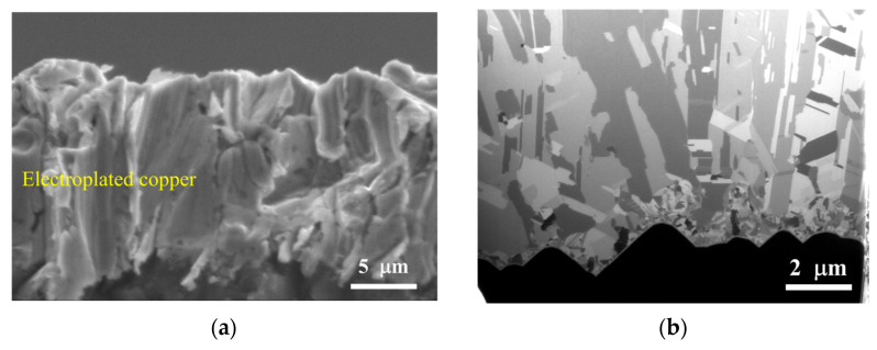
This research, which involved a comprehensive methodology, including depositing electroplated copper on a copper seed layer and Al-doped ZnO (AZO) thin films on textured silicon substrates using DC magnetron sputtering with varying substrate heating, has yielded significant findings. The study thoroughly investigated the effects of substrate temperature (Ts) on copper adhesion strength and morphology using the peel force test and electron microscopy. The peel force test was conducted at angles of 90°, 135°, and 180°. The average adhesion strength was about 0.2 N/mm for the samples without substrate heating. For the samples with substrate heating at 100 °C, the average peeling force of the electroplated copper film was about 1 N/mm. The average peeling force increased to 1.5 N/mm as the substrate heating temperature increased to 200 °C. The surface roughness increases as the annealing temperature of the Cu/AZO/Si sample increases. These findings not only provide a reliable and robust method for applying AZO transparent conductive films onto silicon solar cells but also underscore its potential to significantly enhance the efficiency and durability of solar cells significantly, thereby instilling confidence in the field of solar cell technology.
Keywords: Al-doped ZnO (AZO); adhesion strength; electroplated copper; textured silicon.
Conflict of interest statement
Author Wen-Jauh Chen was employed by the company JBAO Technology Ltd. The remaining authors declare that the research was conducted in the absence of any commercial or financial relationships that could be construed as a potential conflict of interest.
Figures


References
-
- Lin H., Yang M., Ru X., Wang G., Yin S., Peng F., Hong C., Qu M., Lu J., Fang L., et al. Silicon heterojunction solar cells with up to 26.81% efficiency achieved by electrically optimized nanocrystalline-silicon hole contact layers. Nat. Energy. 2023;8:789–799. doi: 10.1038/s41560-023-01255-2. - DOI
-
- Yoshikawa K., Kawasaki H., Yoshida W., Irie T., Konishi K., Nakano K., Uto T., Adachi D., Kanematsu M., Uzu H. Silicon heterojunction solar cell with interdigitated back contacts for a photoconversion efficiency over 26% Nat. Energy. 2017;2:17032. doi: 10.1038/nenergy.2017.32. - DOI
-
- Allen T.G., Bullock J., Yang X., Javey A., De Wolf S. Passivating contacts for crystalline silicon solar cells. Nat. Energy. 2019;4:914–928. doi: 10.1038/s41560-019-0463-6. - DOI
-
- Boccard M., Antognini L., Cattin J., Dréon J., Lin W., Paratte V., Turkay D., Ballif C. Loss analysis of a 24.4%-efficient front-junction silicon heterojunction solar cell and opportunity for localized contacts. IEEE J. Photovolt. 2023;13:663–671. doi: 10.1109/JPHOTOV.2023.3291050. - DOI
-
- Sharma M., Chaudhary D., Dwivedi N., Sudhakar S., Kumar S. Simulating the Role of TCO Materials, their Surface Texturing and Band Gap of Amorphous Silicon Layers on the Efficiency of Amorphous Silicon Thin Film Solar Cells. Silicon. 2017;9:59–68. doi: 10.1007/s12633-015-9331-6. - DOI
LinkOut - more resources
Full Text Sources
