. 2024 Oct 30;14(1):26177.
doi: 10.1038/s41598-024-77460-0.

Effect of electrostatic confinement on the dome-shaped superconducting phase diagram at the LaAlO3/SrTiO3 interface

Affiliations

Effect of electrostatic confinement on the dome-shaped superconducting phase diagram at the LaAlO3/SrTiO3 interface

Paweł Wójcik et al. Sci Rep. .

Abstract

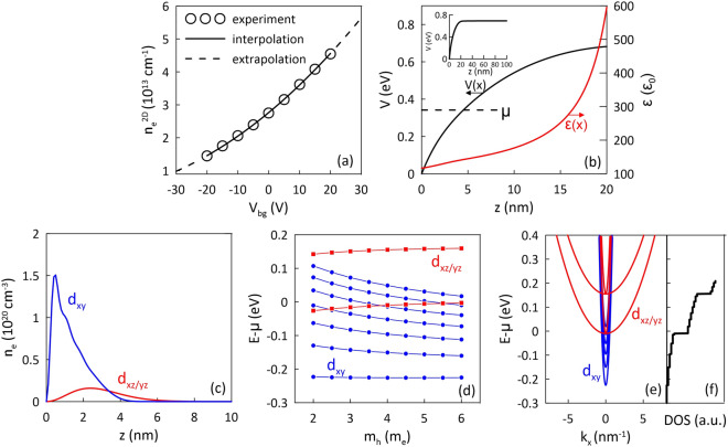
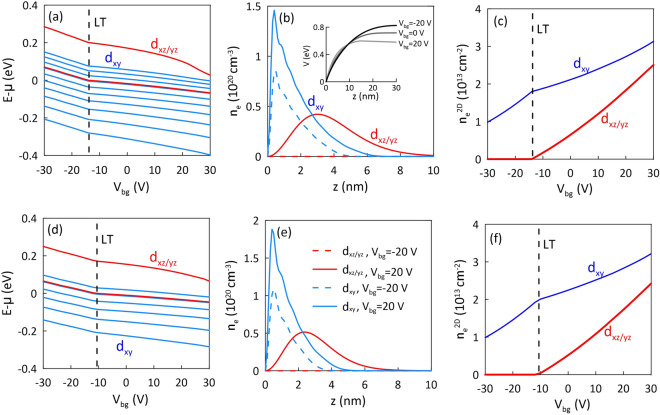
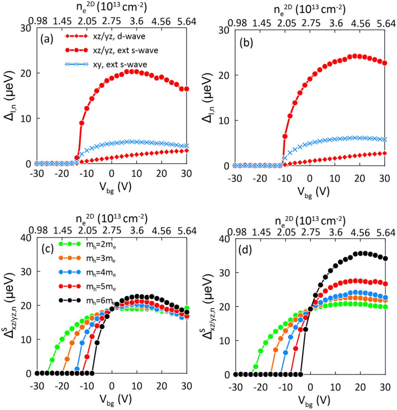
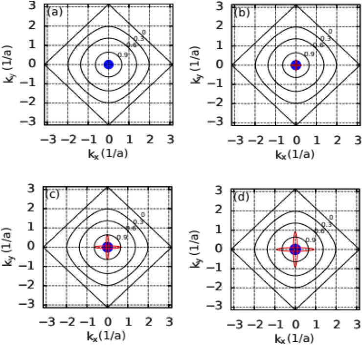
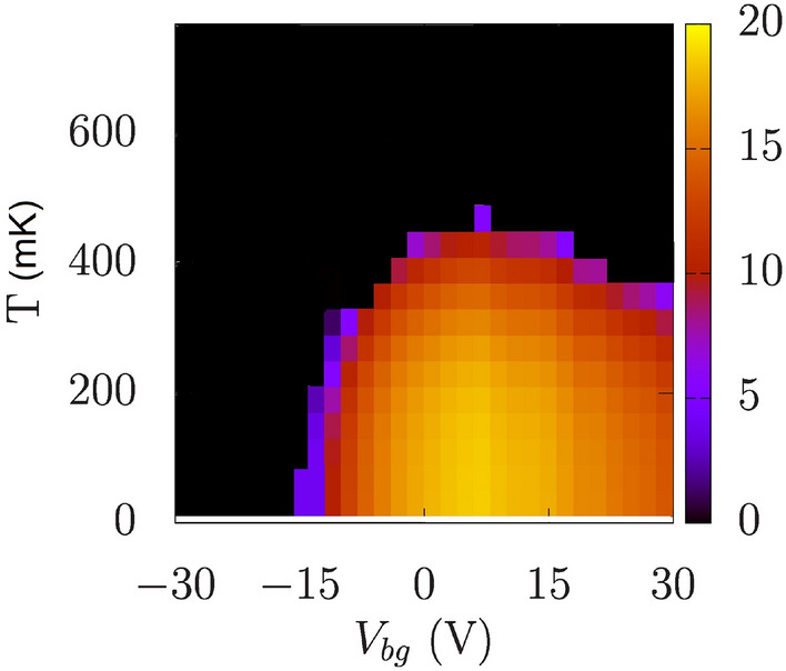
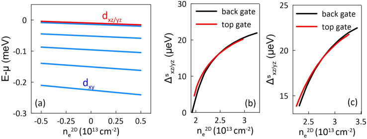
The two-dimensional electron gas (2DEG) at the LaAlO[Formula: see text]/SrTiO[Formula: see text] (LAO/STO) interface exhibits gate-tunable superconductivity with a dome-like shape of critical temperature as a function of electron concentration. This behavior has not been unambiguously explained yet. Here, we develop a microscopic model based on the Schrödinger-Poisson approach to determine the electronic structure of the LAO/STO 2DEG, which we then apply to study the principal characteristics of the superconducting phase within the real-space pairing mean-field approach. For the electron concentrations reported in the experiment, we successfully reproduce the dome-like shape of the superconducting gap. According to our analysis such behavior results from the interplay between the Fermi surface topology and the gap symmetry, with the dominant extended s-wave contribution. Similarly as in the experimental report, we observe a bifurcation effect in the superconducting gap dependence on the electron density when the 2DEG is electrostatically doped either with the top gate or the bottom gate. Our findings explains the dome-shaped phase diagram of the considered heterostucture with good agreement with the experimental data which, in turn, strongly suggest the appearance of the extended s-wave symmetry of the gap in 2DEG at the LAO/STO interface.

Keywords: LAO/STO interface; Oxide interfaces; Unconventional superconductivity.


Conflict of interest statement

The authors declare no competing interests.

Figures

Fig. 1
Fig. 1
Results of the Schrödinger–Poisson calculations for formula image and formula image. (a) 2D electron density formula image vs. back-gate voltage formula image extracted from the experimental data (Fig. 3 in Ref.). Experimental points are marked by dots and the line represents the interpolation. The data are extrapolated by formula image V relative to the voltage range of formula image V reported in the experiment - marked by dashed lines. (b) Self-consistent potential V(z) (black line) and relative permittivity formula image (red line) profiles in the close vicinity of the LAO/STO interface. In the inset, the potential profile V(z) is plotted over the entire simulated range with formula image nm. (c) Electron density distribution near the LAO/STO interface, divided into formula image and formula image bands. (d) Dependence of the electronic structure on the electron mass formula image. (e) Dispersion relation E(k) together with the density of states DOS (f). Results in panels (b, c, e, f) evaluated for formula image.
Fig. 2
Fig. 2
Results of the Schrödinger–Poisson calculations under the back-gating. (a, d) Electronic structure vs. back-gate voltage, formula image. (b, e) Electron density profiles near the LAO/STO interface divided into formula image and formula image orbitals, calculated for formula image V and 20 V. In the inset of panel (b), the potential profile V(z) is plotted for formula image V. (c, f) The electron density formula image for the formula image and formula image orbitals on the back gate voltage formula image. Results for formula image (ac) and formula image (df).
Fig. 3
Fig. 3
(a, b) Superconducting energy gap formula image as a function of back-gate voltage, formula image. The upper x axis displays the corresponding 2D electron density extracted from the experimental data (cf. Fig. 3 in Ref.). Panels (c, d) present the dominant extended s-wave component of superconducting gap in the formula image bands for different strength of electronic band anisotropy determined by formula image. Results for (a, c) formula image and (b, d) formula image.
Fig. 4
Fig. 4
Fermi surfaces of the formula image (red) formula image (blue) bands plotted on the map of isolines determined for the extended s-wave symmetry factor corresponding to formula image (gray lines). Results are shown for (a) formula image V, where the superconducting phase is not observed, (b) formula image V, just above the superconductivity onset, (c) formula image V, at the formula image maximum and above the maximum, for (d) formula image V in the regime of decreasing formula image.
Fig. 5
Fig. 5
Superconducting energy gap formula image as a function of back-gate voltage formula image and temperature T. The evaluated critical temperature at the maximum is 450 mK. Results for formula image.
Fig. 6
Fig. 6
(a) Electronic structure as a function of doping with the top gate voltage. Panels (b, c) present the dominant extended s-wave component of superconducting gap for the formula image bands calculated for the bottom (black) and top (red) gating, assuming in the latter case formula image V (b) and formula image V (c).

Similar articles

References

    1. Reyren, N. et al. Superconducting interfaces between insulating oxides. Science317, 1196–1199 (2007). - PubMed
    1. Joshua, A., Pecker, S., Ruhman, J., Altman, E. & Ilani, S. A universal critical density underlying the physics of electrons at the formula image interface. Nat. Commun.3, 1129 (2012). - PubMed
    1. Maniv, E. et al. Strong correlations elucidate the electronic structure and phase diagram of formula image interface. Nat. Commun.6, 8239 (2015). - PMC - PubMed
    1. Biscaras, J. et al. Two-dimensional superconducting phase in formula image heterostructures induced by high-mobility carrier doping. Phys. Rev. Lett.108, 247004 (2012). - PubMed
    1. Monteiro, M. et al. Band inversion driven by electronic correlations at the (111) formula image interface. Phys. Rev. B99, 201102 (2019).

LinkOut - more resources