. 2025 Feb;20(2):209-215.
doi: 10.1038/s41565-024-01817-9. Epub 2024 Oct 31.

Universal control of four singlet-triplet qubits

Affiliations

Universal control of four singlet-triplet qubits

Xin Zhang et al. Nat Nanotechnol. 2025 Feb.

Abstract

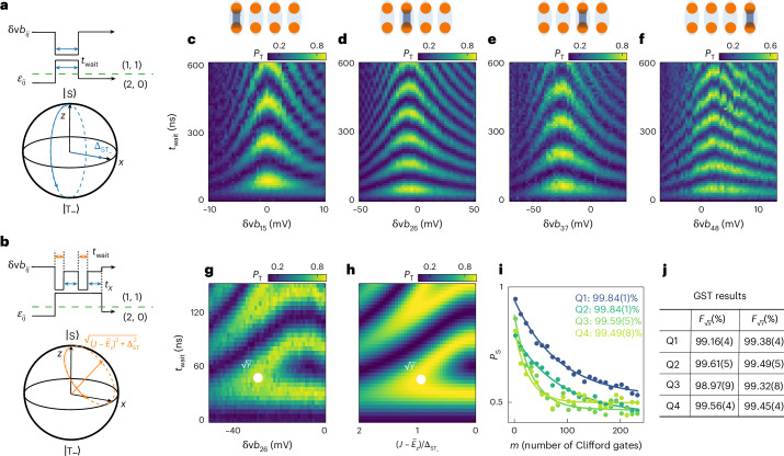
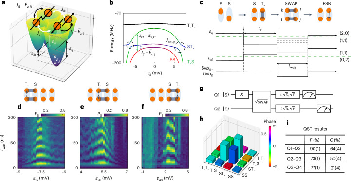
The coherent control of interacting spins in semiconductor quantum dots is of strong interest for quantum information processing and for studying quantum magnetism from the bottom up. Here we present a 2 × 4 germanium quantum dot array with full and controllable interactions between nearest-neighbour spins. As a demonstration of the level of control, we define four singlet-triplet qubits in this system and show two-axis single-qubit control of each qubit and SWAP-style two-qubit gates between all neighbouring qubit pairs, yielding average single-qubit gate fidelities of 99.49(8)-99.84(1)% and Bell state fidelities of 73(1)-90(1)%. Combining these operations, we experimentally implement a circuit designed to generate and distribute entanglement across the array. A remote Bell state with a fidelity of 75(2)% and concurrence of 22(4)% is achieved. These results highlight the potential of singlet-triplet qubits as a competing platform for quantum computing and indicate that scaling up the control of quantum dot spins in extended bilinear arrays can be feasible.


Conflict of interest statement

Competing interests: The authors declare no competing interests.

Figures

Fig. 1
Fig. 1. Device and energy spectroscopy.
a, Schematic drawing showing the Ge/SiGe heterostructure and three layers of gate electrodes on top to define the quantum dot ladder and sensing dots: screening gates (purple), plunger gates (red) and barrier gates (green). Ohmic contacts (grey) extend towards the germanium quantum well in which the holes are confined. The aluminium oxide dielectric between different gate layers is omitted for clarity. b, False-coloured scanning electron microscope image of a device nominally identical to that used in the measurements. The eight quantum dots are labelled 1–8 and the four charge sensors to measure the charge states in the quantum dots are labelled STL, STR, SBL and SBR, respectively. The quantum dot potentials are controlled by plunger gates Pi, and the interdot or dot–sensor tunnel couplings are controlled by barrier gates bij or bi, with i or j denoting the corresponding quantum dot number. A schematic of the ladder structure of the quantum dots is shown on top, with Q1–Q4 formed by vertical DQDs. ce, The energy levels of two-spin states in a DQD as a function of energy detuning εij between dot i and j with J(εij=0)<E¯z(c),J(εij=0)=E¯z(d),J(εij=0)>E¯z(e). The dashed black circles denote the positions of S–T anticrossings. fi, The measured energy spectra that probe the positions of the S–T anticrossings as a function of the detuning (εij) and the barrier gate voltage (vbij) for the vertical DQDs 1–5 (f), 2–6 (g), 3–7 (h) and 4–8 (i) at B = 5 mT. The colour scale shows the measured spin triplet probability PT after initializing a vertical DQD in a singlet state (in (0,2) or (2,0)) and applying a gate voltage pulse (20 ns ramp in, 50 or 60 ns wait time, 0 ns ramp out to the PSB regime for readout) to the detuning shown on the horizontal axis, for different vbij. The 20 ns ramp-in time is used to ensure adiabaticity with respect to the tunnel coupling (2 GHz), while maintaining diabaticity relative to the S–T anticrossing. The wait time is close to a π rotation to obtain a sizable triplet probability. The cartoons on top of the panels fi represent the eight dots, and the dark grey line indicates which exchange coupling is active in the panel below.
Fig. 2
Fig. 2. Universal single-qubit control of four singlet–triplet qubits.
a,b, The pulse schemes used for x-axis control (a) and y-axis control (b). In the experiments, the detuning pulse in a and b has a 20 ns ramp (not shown) from (2,0) to (1,1), similar to the pulse used for the energy spectroscopy. cf, Experimental results for x-axis rotations of Q1 (c), Q2 (d), Q3 (e) and Q4 (f), showing measured triplet probabilities PT as a function of twait and the corresponding barrier voltage δvbij. g, Measured PT for the sequence shown in b as a function of twait and the barrier voltage change δvb26. The position where Y is properly calibrated is indicated by a white dot. h, The numerically computed PT as a function of twait and the ratio of the z-axis component to the x-axis component, (JE¯z)/ΔST. The parameters used for the calculation are extracted from g. i, Single-qubit RB data for Q1–Q4, with PS the measured probabilities of the target state. The 95% confidence intervals based on statistical fluctuations are smaller than the data points. The numbers in the legend are the extracted average gate fidelities, which are obtained from the Clifford gate fidelities using a ratio of 3.625 (see Extended Data Table 1 for the detailed gate decomposition). The errors represent the 68% confidence intervals (Methods). j, Table showing the single-qubit gate fidelities of Q1–Q4 measured by GST. The errors represent the 95% confidence intervals computed using the Hessian of the log-likelihood function. All the data above are measured at B = 5 mT.
Fig. 3
Fig. 3. Two-qubit interactions across the quantum dot ladder.
a, A representation of two connected DQDs. The S–T qubits have a splitting of JijE¯z,ij and JklE¯z,kl (neglecting ΔST), which are controlled by the detunings εij and εkl, respectively. The qubit–qubit coupling Jcoup is an average of Jik and Jjl between the corresponding dots, which are controlled by εik and εjl. b, The energy levels of two-qubit states, where we fix εkl to be positively large and scan εij. At the positions where JijE¯z,ij equals JklE¯z,kl, an anticrossing with a gap Jcoup forms (black dashed circles), which can be used to induce SWAP oscillations between ST and TS. The parameters used in this calculation are based on the experimental results for Q3–Q4 shown in Supplementary Fig. 4c. c, The pulse scheme for SWAP operations. We start in (0,2) or (2,0), at large positive or negative detuning, and diabatically pulse one qubit to (1,1) at modest detuning such that it remains in S, and pulse the other qubit to zero detuning where a π rotation for a time tX takes it to T (other qubits are either initialized to singlets by pulsing back and forth to (0,2) or (2,0), or remain in the (1,1) regime all the time). At this point, the qubits are set to ST or TS. Next, we pulse the detunings of both qubits to make their energies resonant, while at the same time activating Jik and Jjl. This will kickstart SWAP oscillations between the two qubits. The dashed lines in the pulse of εij show that we scan the detuning of one qubit to find the condition for SWAP operations. After an evolution time twait, we pulse the detunings to the PSB readout configuration for one of the qubits. df, The experimental results of SWAP oscillations, showing measured singlet probabilities PS as a function of operation time twait and the detuning voltage εij for Q1–Q2 (d), Q2–Q3 (e) and Q3–Q4 (f). The initial states of two qubits (before the SWAP oscillations) are denoted on the top, and the qubit pair that is read out is indicated by the dashed arrow showing the readout pulse direction. g, The quantum circuit used to create a generalized Bell state between Q1 and Q2 and to characterize it via QST. h, Measured two-qubit density matrix of Q1–Q2, after removal of SPAM errors and using maximum-likelihood estimation (MLE). i, State fidelities and concurrence estimated from the density matrices of the Bell states of Q1–Q2, Q2–Q3 and Q3–Q4. The errors show the uncertainty with 68% confidence intervals (Methods). The data in panels df and h,i are measured at B = 5 mT (see Supplementary Note V for additional data taken at B = 10 mT).
Fig. 4
Fig. 4. Implementation of a quantum circuit for entanglement generation and quantum state transfer.
a, Quantum circuit with all the qubits initialized into the singlet. An X gate (32 ns) rotates Q2 into a triplet state, and a SWAP interaction for a variable time tSWAP periodically produces entanglement between Q1 and Q2. Two subsequent SWAP gates (30 ns and 24 ns) transfer the state of Q2 to Q4 and a final single-qubit rotation of Q4 for a variable time tQ4 is followed by Q4 readout. The delay time between each quantum gate is set to zero. For more details, see Supplementary Note VI. b,c, Experimental (b) and numerical (c) results after running the quantum circuit shown in a, with triplet probabilities PT of Q4 shown as a function of tSWAP and tQ4. The coloured arrows in b show the positions of the linecuts in d. d, Linecuts from a showing triplet probabilities PT of Q4 as a function of control time tQ4, with tSWAP = 0, 4 and 7 ns (from bottom up). The data are vertically shifted by 0.5 for clarity. The 95% confidence intervals based on statistical fluctuations are smaller than the data points. All the data above are measured at B = 10 mT.
Extended Data Fig. 1
Extended Data Fig. 1. Charge stability diagrams and Pauli spin blockade.
a-d, Charge stability diagrams for DQD 1-5 (a), 2-6 (b), 3-7 (c), and 4-8 (d), respectively. a and b are recorded using the sensor SBL while c and d are recorded using the sensor SBR. Hole numbers inside the relevant charge stability regions are indicated, showing all the DQDs can be emptied to (0,0). e-h, Charge stability diagrams measured by scanning the detuning εij and the overall chemical potential μij of the DQD. The PSB regions inside the (2, 0) or (0, 2) area are indicated by solid white triangles and trapezoids. For outer DQD 1-5 and 4-8, we find PSB by pulsing ε15 and ε48 from (1,1) to (2,0) and (0,2), where within a triangular region an electron tunnels between the dots starting from the S(1, 1) but no tunnelling occurs from T0(1, 1), T(1, 1) and T+(1, 1) due to PSB. For inner DQD 2-6 and 3-7, we swap their spin states to those of DQD 5-6 and 7-8 where the sensor signals are stronger. i,j, Illustration of PSB using the energy levels in the quadruple quantum dot plaquette for DQD 2-6 (i) and 3-7 (j), respectively. The hole numbers are indicated as n1,n2n5,n6 for i and n3,n4n7,n8 for j, and the subscripts S and T show the two-spin states of holes in the quantum dots indicated by bold numbers, respectively. The solid arrows show fast spin-conserving tunnelling while the dashed arrows show suppressed tunnelling due to PSB. Here we take pair 2-6 as an example to explain the readout process of the inner spin pairs. First, we align DQD 1-5 at the charge stability boundary between (2,0) and (2,1), as shown by the white dot in e, and then pulse ε26 from negative to positive. We subsequently find a shaded region between (0,1) and (0,2) in the diagram for DQD 2-6, which is caused by PSB in DQD 5-6. The mechanism is shown in i: when we pulse DQD 2-6 to the point where S(0, 2) is lower in energy than (0, 1), the holes in DQD 2-6 moves across to DQD 5-6, irrespective of the spin states. Subsequently, the conventional PSB mechanism in DQD 5-6 allows S(1, 1) to transition to S(0, 2), while the triplets T(1, 1) have to remain in the (1,1) charge state. In this way, we indirectly realize spin-to-charge conversion for the two spins initially in DQD 2-6. Actually, S(1, 1) in DQD 2-6 can also directly tunnel to S(0, 2) inside the same DQD, as seen by the curved arrow in i. The mechanism to measure DQD 3-7 is analogous.
Extended Data Fig. 2
Extended Data Fig. 2. Data of two-axis qubit control around the x- and z-axis, measured at B = 10 mT.
a,b, Pulse scheme and Bloch sphere illustration of x-axis and z-axis evolution of ST qubits. The straight blue and orange arrows show the corresponding rotation axis. The x-axis rotations are set by the ST coupling, ΔST. For large J such that JE¯zΔST, the rotation axis tilts towards the z-axis. The rotation is never exactly around the z-axis due to the presence of a finite ΔST, yet, sufficiently orthogonal control is possible when (JE¯z)ΔST. In b, we illustrate a Ramsey-like pulse sequence used to demonstrate z-axis control. We first initialize the qubit into a singlet, perform a π/2 rotation around the x-axis of duration tπ/2, and then change J diabatically by pulsing the corresponding barrier gate by an amount δvbij to implement a z-axis rotation. Finally, we perform another π/2 operation around the x-axis and project the qubit into the ST basis for spin readout. c-f, Experimental results for x-axis rotations of each qubit, showing measured triplet probabilities PT as a function of twait and the detuning voltage εij. g-j, Experimental results for z-axis rotations of each qubit, showing PT as a function of twait and the barrier voltage change δvbij. The oscillation frequency is given by fST=(JE¯z)2+ΔST2/h, where h is Planck’s constant. We note that the outer two barrier gates vb15 and vb48 have a stronger effect on the corresponding Jij than the inner barrier gates vb26 and vb37. This may be explained by additional residual resist below the inner barrier gates, which are fabricated in the last step, and by the different fan-out routing for the outer barrier gates (see Fig. 1a,b in the main text). Within the tuning range of the barrier gate, the highest ratio (JE¯z)/ΔST amounts to around 20 for the outer qubits Q1 and Q4 and about 10 for the inner qubits Q2 and Q3 (see Supplementary Information IV for more details).
Extended Data Fig. 3
Extended Data Fig. 3. Decoherence times of the qubits under control.
a, Measured triplet probabilities PT of long-time evolutions around the x-axis for Q1–Q4 at B=5 mT. b, Measured singlet probabilities PS as a function of the evolution time twait at the centre of the chevron patterns of the SWAP oscillations for each pair of qubits at B=5 mT. The data of a and b are fitted with a function of the form PT=P0+Acos(2πft+ϕ)exp[(t/T*)β], where P0, A, β, f, T* are fitting parameters. Here f refers to the oscillation frequency, T* refers to Tx*, the coherence time under x-axis rotations, or TQiQj*, the coherence time under SWAP oscillations between adjacent qubits. Furthermore, the parameter β determines the shape of the decay envelope, and the fitted values are shown in the inset. β provides insight into the noise spectrum within the system: when quasi-static or low-frequency noise dominates, β = 2, leading to Gaussian decay; whereas when high-frequency noise prevails, β = 1, resulting in exponential decay. The extracted β for the x-axis rotations of Q1-Q3 and all the SWAP oscillations are close to 2, indicating the dominance of low-frequency noise in this system. Notice the large value of β for the x-axis rotations of Q4 may result from the fitting error. The errors represent the 68% confidence intervals obtained from fitting.
Extended Data Fig. 4
Extended Data Fig. 4. Coherent control of singlet-triplet states under different conditions and the average g-factor.
a, Pulse scheme to measure ST and ST0 oscillations. A square pulse is used with a ramp-in time tramp and waiting time twait. b, Measured triplet probabilities of DQD 4-8 as a function of twait and the barrier voltage amplitude δvb48 with tramp = 20 ns. As mentioned in the main text, a block pulse along the detuning axis with 20-nanosecond ramp time (tramp) from (0,2) to (1,1) is adiabatic with respect to the tunnel coupling but diabatic with respect to the ST anticrossing. Therefore, we can drive x-rotations of ST qubits when the pulse amplitude reaches zero detuning with J(εij=0)~Ez¯ (see Fig. 1d in the main text). However, when we increase the barrier voltage change δvb48 until J(εij=0)<Ez¯ (δvb48 ~ 40 mV), the ST anticrossings appear away from zero detuning (see Fig. 1c in the main text), thus the same pulse does not produce x-axis oscillations of the ST qubit. Moreover, under this condition, the ST0 splitting is reduced and the 20-nanosecond ramp time eventually becomes diabatic with respect to the ST0 splitting. As a result, the singlet state will rotate between the S and T0 states under the Zeeman energy difference between the two dots ΔEz. c, Measured triplet probabilities of DQD 4-8 as a function of twait and tramp with δvb48 = 40 mV. When tramp is small, the observed oscillations are between S and T0; however, when tramp is increased until the pulse is adiabatic with respect to the ST0 splitting (over 100 ns), the ST0 oscillations can no longer be observed. Such a long ramp time can rotate the initial state to a superposition state between S and T states, and z-axis rotations of the ST qubit become visible. Therefore, we also observe a transition of ST0 oscillations and ST oscillations as a function of tramp in the figure. d, The rotation frequency fST of each qubit as a function of the magnetic field strength B. When the external magnetic field strength is varied while keeping the gate voltages fixed, the frequency of these ST oscillations increases nearly linearly with the field due to the contribution from Zeeman energy in fST. From the slope, we extract g¯ij for the four qubits as shown in the inset. The errors represent the 68% confidence intervals obtained from fitting. The data are acquired using the fast Fourier transform (FFT) of time-domain oscillations in e-h. e-h, Measured singlet probabilities PS of Q1 (i), Q2 (j), Q3 (k), and Q4 (l) as a function of twait and magnetic field strength B. The rotations are induced using the pulse scheme of panel a with tramp = 100 ns.
Extended Data Fig. 5
Extended Data Fig. 5. Coherent control of ST0 states and g-factor differences.
a-c, Measured singlet probabilities PS as a function of twait and the magnetic field strength B for Q1 (c), Q2 (d), and Q4 (e) during ST0 oscillations. Here tramp is set to zero and the barrier gate voltage is set such that J(εij=0)<Ez¯ to suppress unwanted ST oscillations. d-f, The fast Fourier transforms of the data in a-c, with a signal that can be line-fitted using the g-factor difference Δgij (inset) of two dots. The errors represent the 68% confidence intervals obtained from fitting. For Q3, we didn’t find ST0 oscillations, which may be because the corresponding Δg is too low to detect.
Extended Data Fig. 6
Extended Data Fig. 6. Results of single-qubit gate set tomography.
a-h Single-qubit Pauli transfer matrices (PTM) of the X gate (a-d) and Y gate (e-h) for Q1–Q4 (from left to right) obtained from gate set tomography. i-l, Estimated state preparation and measurement (SPAM) error probabilities from GST results for Q1–Q4, using the same method as used in. We find that the SPAM errors of Q2 and Q3 are worse than those of Q1 and Q4. There are two reasons. Firstly, the indirect PSB mechanism is more sensitive to the readout point we chose and the idling point of the other qubit. In particular, the readout fidelity of the triplet is lower when triplet relaxation is faster at the readout point. Secondly, the slower tunnelling rate from (0,2) or (2,0) to (1,1) causes an initialization error in some cases. Also, the instability of the charge sensor can contribute to the readout error, which makes the readout visibility vary between different measurements.
Extended Data Fig. 7
Extended Data Fig. 7. Sequential readout and joint probabilities of two qubits under SWAP oscillations.
a,b, Sequentially measured probabilities PSS, PTS, PST and PTT of Q2 and Q3 as a function of twait and the detuning of Q3, ε37, after initializing Q2–Q3 into TS (a) and SS (b). The data is acquired at B = 5 mT. In a, the out-of-phase signals in PTS and PST observed around ε37 = 1.5 mV are the result of the SWAP oscillations between these two qubits. A similar signal to PTS but with lower visibility is observed in PSS, which can be explained by the higher triplet readout error for Q2 than for Q3. The sequential readout is achieved by pulsing the barrier gate δvb26 to -60 mV, where we measure Q3 first for a duration of 20 μs and simultaneously keep Q2 in the centre of (1,1) with sufficiently large J, where the Hamiltonian eigenbasis corresponds to the qubit readout basis,,. In the next step of the sequence, Q2 is measured. In panel b, we do not observe any apparent leakage to TT but only see signs of single-qubit rotations at low detunings. This is expected given that, in this regime, the states TT are far away in energy from the other states (see Fig. 3b in the main text).
Extended Data Fig. 8
Extended Data Fig. 8. Quantum gate circuit and results for quantum state tomography of the Bell states.
a,c,f,i, Quantum circuit used to prepare and characterize a Bell state for different qubit pairs. In a, we plot the details of the single-qubit basis changes after the generation of the Bell state, where we apply a fixed wait time before performing gates on Q2 to keep its phase consistent through all the experiments. In c, SWAP gates are used to transfer the state of Q2 to Q1 and that of Q3 to Q4. Next Q1 and Q4 are measured simultaneously using two sensors. In f, two consecutive SWAP gates are used to transfer Q3 to Q1. Next Q1 and Q4 are measured simultaneously using two sensors as well. In i, the quantum information is transferred from Q2 to Q4 before performing the single-qubit gates for basis changes. This allows us to quantify the entanglement between Q1 and Q4 after state transfer. d,g,j, Two-qubit density matrices obtained from the corresponding quantum circuit after removal of measurement errors and using MLE for Q2–Q3 (d), Q3–Q4 (g) and Q1–Q4 (j) (Fig. 3h shows the density matrix for Q1–Q2). Measurement errors were removed based on the SPAM matrices. These matrices include not only measurement errors but also initialization errors, hence we are overcorrecting. The fact that initialization errors for most qubits were much smaller than measurement errors combined with the fact that MLE forces the resulting density matrix to be physical, helps ensure a reliable outcome. If we don’t attempt to remove readout errors, the density matrices show state fidelities and concurrences of 71.3(6)% and 9(2)% for Q1–Q2, 64.2(6)% and 10(2)% for Q2–Q3, 64.6(7)% and 0(0)% for Q3–Q4 and 64.4(9)% and 0(0)% for Q1–Q4. The errors represent the 68% confidence intervals (Methods). b,e,h,k, SPAM matrices used in the quantum state tomography analysis of Q1–Q2 (b), Q2–Q3 (e), Q3–Q4 (h) and Q1–Q4 (k). The SPAM matrices of Q1–Q2 and Q1–Q4 were measured directly by initializing them to the indicated states and measuring the corresponding pair in a single-shot manner. For Q2–Q3 or Q3–Q4, we initialized the qubits to the indicated states and measured the state of Q1–Q4 after the SWAP operations. These SPAM matrices do include errors from the SWAP operations.
Extended Data Fig. 9
Extended Data Fig. 9. Measurement sequence and results of two-qubit gate set tomography.
a, Illustration of the gate voltage pulses for a two-qubit circuit. Performing a single-qubit gate in the two-qubit space is nontrivial since during the time one qubit is undergoing an operation, the idling qubit could suffer from unwanted rotations and crosstalk. To solve this problem, we pulse the idle qubit to an operating point where it completes a 2π rotation during the time needed to operate on the other qubit (see Supplementary Information VIII for more details). b-e, Measured PTMs obtained from GST for single-qubit gates in the two-qubit space, including XQ1 (b), XQ2 (c), YQ1 (d) and YQ2 (e). f-i, The ideal PTMs from GST for single-qubit gates in the two-qubit space, including XQ1 (f), XQ2 (g), YQ1 (h) and YQ2 (u). j, SPAM error matrix of the measured two qubits estimated from GST, using the same method as used in. k, The PTM of the standard SWAP based on an isotropic Heisenberg exchange Hamiltonian. l, The experimentally measured PTM, Mexp, obtained from GST. m, The theoretical PTM, Mthe, of the SWAP-style gate obtained by fitting the experimentally measured PTM, Mexp, with a PTM generated by Eq. (28) in Supplementary Information VII (the fitted parameters are given there). The Hamiltonian Eq. (28) includes effects of spin–orbit coupling that are left out in the Hamiltonian of Eq. (2) of the main text. The fidelity of the SWAP-style gate is obtained from F=1d+1(Tr[Mthe1Mexp]/d+1), where d = 2N is the dimension of the Hilbert space, and N refers to the number of qubits.

References

    1. Vandersypen, L. et al. Interfacing spin qubits in quantum dots and donors—hot, dense, and coherent. npj Quantum Inf.3, 34 (2017).
    1. Heinrich, A. J. et al. Quantum-coherent nanoscience. Nat. Nanotechnol.16, 1318–1329 (2021). - PubMed
    1. Gonzalez-Zalba, M. et al. Scaling silicon-based quantum computing using CMOS technology. Nat. Electron.4, 872–884 (2021).
    1. Chatterjee, A. et al. Semiconductor qubits in practice. Nat. Rev. Phys.3, 157–177 (2021).
    1. Stano, P. & Loss, D. Review of performance metrics of spin qubits in gated semiconducting nanostructures. Nat. Rev. Phys.4, 672–688 (2022).

LinkOut - more resources