. 2024 Nov 13;24(45):14191-14197.
doi: 10.1021/acs.nanolett.4c02913. Epub 2024 Nov 1.

Electron-Beam Writing of Atomic-Scale Reconstructions at Oxide Interfaces

Affiliations

Electron-Beam Writing of Atomic-Scale Reconstructions at Oxide Interfaces

Greta Segantini et al. Nano Lett. .

Abstract

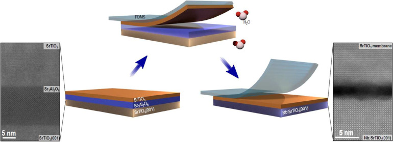
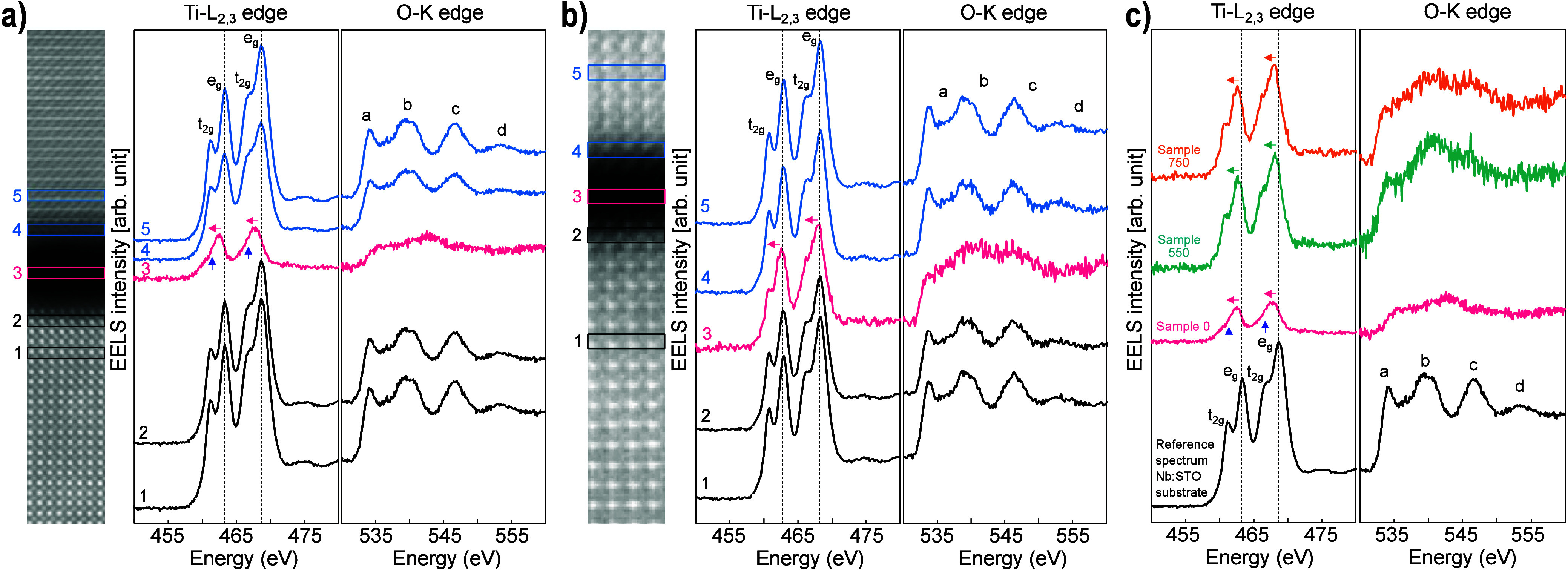
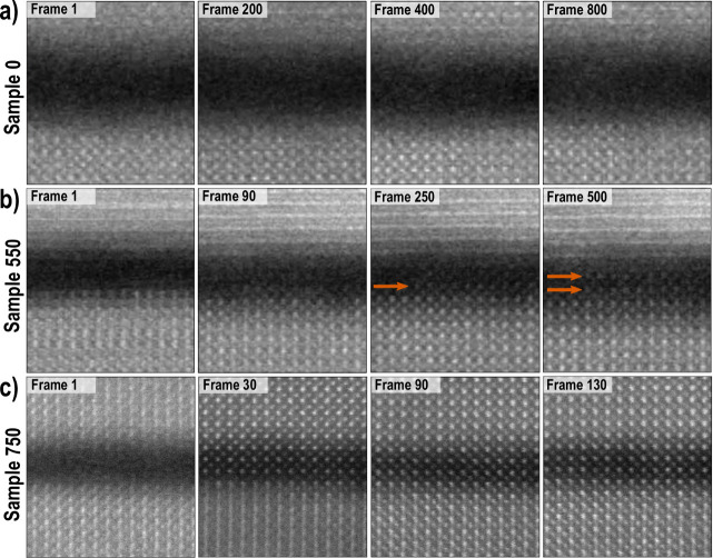
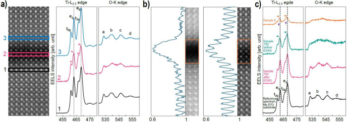
The epitaxial growth of complex oxides enables the production of high-quality films, yet substrate choice is restricted to certain symmetry and lattice parameters, thereby limiting the technological applications of epitaxial oxides. In comparison, the development of free-standing oxide membranes gives opportunities to create novel heterostructures by nonepitaxial stacking of membranes, opening new possibilities for materials design. Here, we introduce a method for writing, with atomic precision, ionically bonded crystalline materials across the gap between an oxide membrane and a carrier substrate. The process involves a thermal pretreatment, followed by localized exposure to the raster scan of a scanning transmission electron microscopy (STEM) beam. STEM imaging and electron energy-loss spectroscopy show that we achieve atomically sharp interface reconstructions between a 30-nm-thick SrTiO3 membrane and a niobium-doped SrTiO3(001)-oriented carrier substrate. These findings indicate new strategies for fabricating synthetic heterostructures with novel structural and electronic properties.

Keywords: in-situ e-beam writing; interface; ionic bonding; oxide membranes; perovskites.


Conflict of interest statement

The authors declare no competing financial interest.

Figures

Figure 1
Figure 1
Schematic of the membrane fabrication process: The Sr3Al2O6 sacrificial layer and the SrTiO3 membrane were synthesized using PLD. Subsequently, a PDMS sheet was applied to the surface of the SrTiO3 layer, and the entire structure was immersed in deionized water. Following the dissolution of the Sr3Al2O6 layer, the resulting SrTiO3 membrane was transferred onto the Nb:SrTiO3(001) substrate. HAADF STEM cross-sectional images of the heterostructure SrTiO3(001)/Sr3Al2O6/SrTiO3 before lift-off and of the SrTiO3 membrane transferred onto the Nb:SrTiO3(001) substrate are shown on the left and on the right, respectively. In the latter, an interface gap of ∼2 nm between the SrTiO3 membrane and the Nb:SrTiO3(001) substrate is distinguishable.
Figure 2
Figure 2
Effect of annealing of the SrTiO3 membrane on Nb:SrTiO3(001) substrate. (a) STEM-EELS analysis of Sample 0. From left to right: HAADF cross-sectional image of Nb:SrTiO3(001) substrate/SrTiO3 membrane, background-subtracted Ti-L2,3 and O-K edges extracted from #1 Nb:SrTiO3(001) substrate, #2 Nb:SrTiO3(001) substrate near the bottom interface, #3 center of the gap, #4 SrTiO3 membrane near the top interface, and #5 SrTiO3 membrane. The Ti-L2,3 and O-K edges in spectrum #3 reveal a clear change compared to the crystalline SrTiO3. In particular, the splitting of the Ti L3 and L2 peaks observed in spectra #1, #2, #4, and #5, that indicates a Ti4+ oxidation state, is no longer visible, suggesting a change in Ti valence from 4+ to 2+ . (b) STEM-EELS analysis of Sample 750: spectrum #3 of Ti-L2,3 edge indicates that Ti has shifted toward 4+ valence; the first fine structure peak of the O-K edge has also moved to a lower energy compared to gap spectrum #3 in (a). (c) Comparison of Ti-L2,3 and O-K edges obtained from Sample 0, Sample 550, and Sample 750 extracted in the center of the gap together with a reference from the Nb:SrTiO3(001) substrate. The evolution of the Ti-L2,3 edges as a function of the annealing temperature demonstrates a clear change in Ti valence state. All the displayed spectra are background-subtracted, equivalently normalized by substrate intensities, and aligned on the energy-loss axis using the O-K edge onset energy (532 eV). Note that, for compactness, the HAADF images are cropped from the full width of the original mapped areas. The EEL spectra are integrated from the full map width.
Figure 3
Figure 3
Effect of STEM-EDXS raster scan conditions on Nb:SrTiO3(001) substrate/SrTiO3 membrane system, showing the evolution of the interface gap as a function of the acquired number of frames. (a) Sample 0: no evident changes are observed after 800 frames. (b) Sample 550, ordered atomic structure emerges within the gap after 250 frames. At the final frame 500, the gap is largely filled with crystalline structure. (c) Sample 750, crystal structure completely fills the gap after 30 frames. By frame 130, the cation sites of substrate and membrane have also come into alignment.
Figure 4
Figure 4
Effect of the EDXS condition e-beam raster scan on Sample 750. (a) STEM-EELS analysis after the EDXS raster scanning that is shown in Figure 3c. From left to right, the HAADF image, Ti-L2,3 edge, and O-K edges acquired from the Nb:SrTiO3(001) substrate, the gap, and the membrane. The HAADF image depicts clear atomic columns within the gap. EEL spectral features of the Ti-L2,3 and O-K edges closely resemble those observed in the Nb:SrTiO3(001) substrate and membrane. (b) Ti-L edge integrated signal from EELS map acquired from the initial “pristine” area, and from the same area after the EDXS raster scanning shown in Figure 3c. The consistent intensity of the Ti integrated signal indicates no mass loss or gain of Ti atoms within the gap during the structural reorganization to a crystalline structure. The HAADF images are cropped from the full width of the original mapped areas. (c) Comparison of EEL spectra from the center of the interface gap for as-transferred, 750 °C annealed, and 750 °C annealed–EDXS raster scanned, together with a reference spectrum from the Nb:SrTiO3(001) substrate. Displayed EEL spectra were processed as for Figure 2.

References

    1. Chambers S. A. Epitaxial growth and properties of doped transition metal and complex oxide films. Adv. Mater. 2010, 22, 219–248. 10.1002/adma.200901867. - DOI - PubMed
    1. Koster G.; Huijben M.; Rijnders G.. Epitaxial Growth of Complex Metal Oxides; Woodhead Publishing: 2015.
    1. Cen C.; Thiel S.; Mannhart J.; Levy J. Oxide nanoelectronics on demand. Science 2009, 323, 1026–1030. 10.1126/science.1168294. - DOI - PubMed
    1. Li W.; Shi J.; Zhang K. H. L.; MacManus-Driscoll J. L. Defects in complex oxide thin films for electronics and energy applications: challenges and opportunities. Mater. Horiz. 2020, 7, 2832–2859. 10.1039/D0MH00899K. - DOI
    1. Liu Q.; Gao S.; Xu L.; Yue W.; Zhang C.; Kan H.; Li Y.; Shen G. Nanostructured perovskites for nonvolatile memory devices. Chem. Soc. Rev. 2022, 51, 3341–3379. 10.1039/D1CS00886B. - DOI - PubMed

LinkOut - more resources