Review
. 2025 Jul;21(28):e2403089.
doi: 10.1002/smll.202403089. Epub 2024 Nov 2.

Tailored Growth of Transition Metal Dichalcogenides' Monolayers by Chemical Vapor Deposition

Affiliations
Review

Tailored Growth of Transition Metal Dichalcogenides' Monolayers by Chemical Vapor Deposition

Andrey Turchanin et al. Small. 2025 Jul.

Abstract

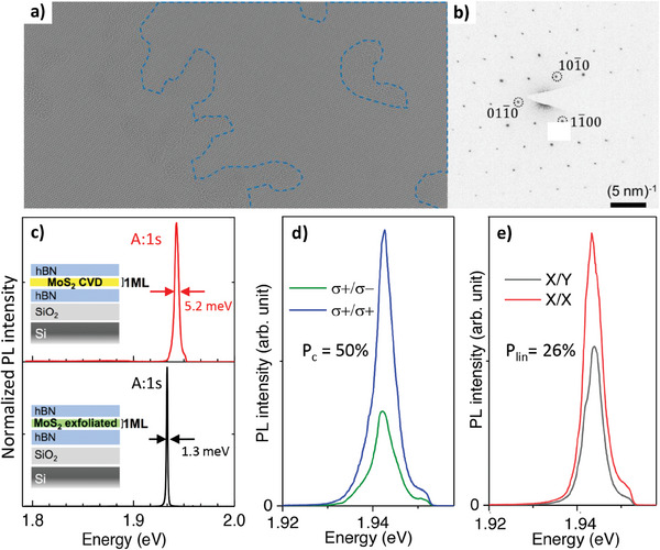
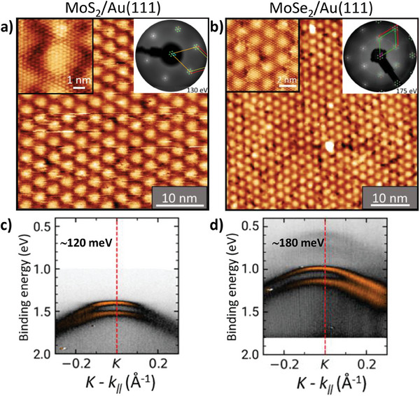
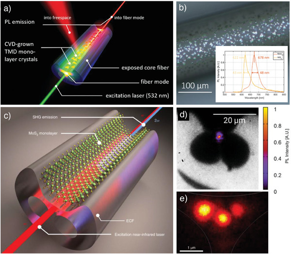
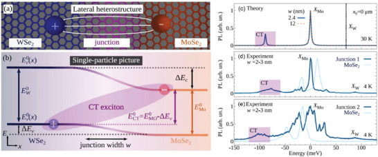
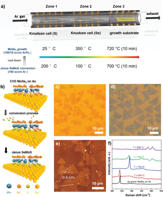
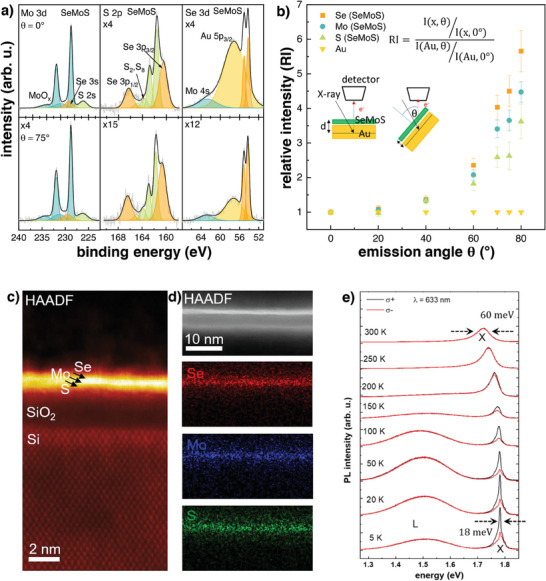
Here, results on the tailored growth of monolayers (MLs) of transition metal dichalcogenides (TMDs) are presented using chemical vapor deposition (CVD) techniques. To enable reproducible growth, the flow of chalcogen precursors is controlled by Knudsen cells providing an advantage in comparison to the commonly used open crucible techniques. It is demonstrated that TMD MLs can be grown by CVD on large scale with structural, and therefore electronic, photonic and optoelectronic properties similar to TMD MLs are obtained by exfoliating bulk crystals. It is shown that besides the growth of the "standard" TMD MLs also the growth of MLs that are not available by the exfoliation is possible including examples like lateral TMD1-TMD2 ML heterostructures and Janus TMDs. Moreover, the CVD technique enables the growth of TMD MLs on various 3D substrates on large scale and with high quality. The intrinsic properties of the grown MLs are analyzed by complementary microscopy and spectroscopy techniques down to the nanoscale with a particular focus on the influence of structural defects. Their functional properties are studied in devices including field-effect transistors, photodetectors, wave guides and excitonic diodes. Finally, an outlook of the developed methodology in both applied and fundamental research is given.

Keywords: 2D materials; chemical vapor deposition; devices; structural properties; transition vapor dichalogenides.


Conflict of interest statement

The authors declare no conflict of interest.

Figures

Figure 1
Figure 1
Schematic overview of the TMD ML structures presented in this review.
Figure 2
Figure 2
Schematic diagram of a CVD experimental set up with a) open crucibles for the precursors and with b) Knudsen effusion cells for controlling the precursors flow. Reproduced with permission.[ 93 ] Copyright 2019, IOPscience.
Figure 3
Figure 3
TMD MLs grown by CVD with the Knudsen cells for chalcogen precursors. a) MoS2 on SiO2/Si. Reproduced with permission.[ 93 ] b) WS2 on SiO2/Si. Reproduced with permission.[ 93 ] c) WS2 on sapphire. Reproduced with permission.[ 93 ] Copyright 2019, IOPscience. d) MoSe2 on SiO2/Si. Reproduced with permission.[ 76 ] e) WSe2 on SiO2/Si. Reproduced with permission.[ 76 ] Copyright 2021, Wiley‐VCH GmbH. f) NbSe2 on SiO2/Si.
Figure 4
Figure 4
Characterization of the structural and optical quality of the CVD‐grown MoS2 MLs. a) 60 kV HRTEM atomically resolved image of the suspended monolayer; defect density was calculated on clean areas of the sample, which are framed with the dashed blue line. b) The diffraction pattern shows a high crystallinity sample imaged in panel (a). c) The photoluminescence (PL) emission linewidth of CVD‐grown MoS2 ML (top) and exfoliated one (bottom) encapsulated in hexagonal boron nitride (hBN); λ = 633 nm, T = 4 K. The insets show an optical image the hBN‐encapsulated CVD‐grown MoS2 ML (65 µm × 65 µm) and a scheme of the encapsulation. PL emission from the CVD‐grown MoS2 ML is strongly d) circularly and e) linearly polarized, which exhibits efficient valley polarization and valley coherence. Reproduced with permission.[ 96 ] Copyright 2020, IOP science.
Figure 5
Figure 5
Interlayer excitons in MoS2 bilayer‐grown CVD. Reproduced with permission.[ 98 ] Copyright 2020, Nature Publishing Group. a) Optical microscope images of as‐grown 3R (left) and 2H CVD MoS2 bilayers (right) on SiO2/Si substrate before encapsulation in hBN. b) First derivative of white light reflection spectrum for as‐grown 2H‐bilayer (blue) and as‐grown 3R‐bilayer (red), recorded at T  =  4 K. c) Deterministically assembled 3R and 2H MoS2 homo‐bilayers fabricated by a dry transfer process. d) First derivative of reflectivity spectra collected from three different areas of the artificially stacked 3R (red) and 2H (blue) MoS2 homo‐bilayers recorded at T = 4 K. All samples were encapsulated in high‐quality hBN for optical spectroscopy. e) Schematic of 3R‐stacked bilayers with intralayer excitons (top) compared to 2H‐stacked bilayer where, in addition, intralayer excitons are formed.
Figure 6
Figure 6
Characterization of the structural and optical quality of the CVD‐grown MoS2 and MoSe2 MLs on Au(111). Reproduced with permission.[ 99 ] Copyright 2023, The Royal Society of Chemistry. a) MoS2 STM image (293 K, 0.5 V, 0.5 nA); inset (left): STM image (293 K, 0.5 V, 1.2 nA); inset right: respective LEED pattern. b) MoSe2 STM image (4.2 K, 0.4 V, 50 pA); inset (left): STM image (4.2 K, 1.5 V, 20 pA); inset (right): respective LEED pattern. c,d) ARPES MoS2 and MoSe2 showing spin–orbit splitting of their valence bands at the respective K points.
Figure 7
Figure 7
60 kV HRTEM images of a,b) MoS2 and c,d) WS2. Reproduced with permission.[ 103 ] Copyright 2021, Nature Publishing Group. a) The raw image of MoS2. The area within the white square is magnified in the lower right. Red circles mark the vacancies that are difficult to see even in the magnified image. b) Fourier filtering was applied to remove the frequencies of the MoS2 lattice. In panel (b), the same area like in panel (a) is magnified. Due to the Fourier filtering, the vacancies are better visible (black dots, surrounded by red circles). The same procedure was also applied for WS2. c) Raw image and d) Fourier‐filtered image are shown. Due to the filtering, contamination gets also more visible, outside the framed area; thus, only clean areas were evaluated with certainty for the defect concentration.
Figure 8
Figure 8
Visualization of the band structure spatial fluctuations in a MoS2 ML. Reproduced with permission.[ 103 ] Copyright 2021, Nature Publishing Group. a) STS data obtained at two different positions, marked in panels (b) and (c), on MoS2/hBN/Pt(111) showing the trap states above the valence band and below the conduction band. b,c) STS maps visualizing spatial inhomogeneity of the valence and conduction band, respectively.
Figure 9
Figure 9
Giant persistent photoconductivity (GPPC) in MoS2 ML FETs after irradiation with UV light. Reproduced with permission.[ 103 ] Copyright 2021, Nature Publishing Group. a) Schematic representation of the device and measurement setup. b) The black curve represents the transfer characteristics of MoS2 device before UV irradiation, and the red curve represents the transfer characteristics immediately after UV irradiation (λ = 365 nm) for 5 min with an intensity of 321 mW cm−2. The colored curves represent the transfer characteristics recorded on the following days after UV irradiation. The inset shows an optical microscopy image of the MoS2 FET device. c) The decay of drain current with time at V g = 0 V. The experimental data were fitted (red curves) using a two‐stage exponential decay function to extract the GPPC decay time constants. Calculated decay of photoelectron concentration with time is shown in the inset. d) Schematic representation of band fluctuations in the MoS2 ML. An incident photon excites an electron from the valence to conduction band; due to position‐dependent fluctuations in the band structure, the electrons and holes are spatially separated with a distance of ∆x. µe ( I, D ) correspond to the quasi‐Fermi levels of the equilibrium and photogenerated electrons, respectively.
Figure 10
Figure 10
Patterned growth of TMD MLs. Reproduced with permission.[ 107 ] Copyright 2022, Wiley‐VCH GmbH. a) A polydimethylsiloxane (PDMS) mold is placed on the substrate to form capillaries. b) Filling the capillary channels with precursor solution. c) Drying of the precursor and removal of the mold. d) CVD conversion of the precursors to TMD patterns. e,f) Optical microscopy images of MoS2 and MoSe2 line patterns grown on SiO2/Si substrate by CVD conversion of Na2MoO4 line patterns. g) Electronic and optoelectronic response of the MoS2 MLs. Transfer characteristics of the FET device (in the forward sweep direction) under dark and varying illumination intensities (λ = 635 nm) are shown; the contact pads were defined on an array consisting of four MoS2 line patterns (length ≈ 5 µm, width ≈ 6 µm) as shown in the inset scheme. h) Memtransistor characterization performed on the MoS2 device shown in panel (g); I dsV ds characteristics of the device at various gate voltages.
Figure 11
Figure 11
Electronic and photoelectronic devices based on hybrid organic–inorganic vdW heterojunctions. Reproduced with permission.[ 115 , 118 ] Copyright 2021, Nature Publishing Group and copyright 2021, Wiley‐VCH GmbH, respectivly. a,b) Schematics of ambipolar and anti‐ambipolar devices, respectively, based on MoS2 MLs and OSC nanosheets. c) Transfer curves of the device depicted in panel (a). d) Transfer curves of the devices depicted in panel (b). Schematic of the MoS2 ML/BTBT‐SAM FET device. d) Transfer curves and e) photoresponse of the device depicted in panel (c).
Figure 12
Figure 12
Performance of MoS2 ML FETs on the SiO2 gate dielectric passivated with cyclic olefin copolymer (COC). Reproduced with permission.[ 119 ] Copyright 2023, Wiley‐VCH GmbH. a) Schematic of the device. b) Transfer curves of four devices on 100 nm thick, COC‐passivated, SiO2. c) Subthreshold swing on the bare and passivated substrates with different oxide thickness; the dashed and solid lines are fits including the thermionic limit at infinite capacitance. d) The time‐resolved photocurrent measurements performed under vacuum and illumination by 405 nm lasers.
Figure 13
Figure 13
Lateral heterostructures of TMD MLs and 2D molecular materials via their electron‐irradiation‐induced stretching. Reproduced with permission.[ 120 ] Copyright 2018, Elsevier. a) Schematic of a lateral heterostructure of MoS2 ML and 1 nm thick carbon nanomembrane (CNM). b) HRTEM image showing CNM (top left) and MoS2 (bottom right); the boundary between two materials is marked red. c) Filtered image of panel (b) showing the crystalline MoS2 area (bright) and the amorphous CNM area (dark).
Figure 14
Figure 14
Resonant photonic nanostructures with TMD MLs. Reproduced with permission.[ 125 , 126 , 127 ] Copyright 2019 and 2021, American Chemical Society and copyright 2019, Optica Publishing Group, respectivly. a) Schematic of a MoS2 ML transferred on top a silicon nanocylinder metasurface. b) True‐color optical image on the hybrid structure presented in panel (a). c) Cross‐sectional SEM image of the sample in panel (b) showing a region covered with MoS2 ML. d) Special PL mapping of the hybrid samples with varying diameter, D, of silicon nanocylinders. e) Schematic of SHG in MoS2 ML atop of a resonant silicon metasurface. Left: Top and side views as well as the SEM image. f) Left: White light microscope image from a MoS2 ML crystal on top of a resonant silicon metasurface. Right: SHG intensity map of the sample. g) Design of the pattern with a fork‐like structure. Optical microscope image of the patterned MoS2 ML crystal. Back‐focal plane image of the SHG signal.
Figure 15
Figure 15
CVD‐based functionalization of exposed‐core optical fibers with TMD MLs. Reproduced with permission.[ 95 , 129 ] Copyright 2020, Wiley‐VCH GmbH and copyright 2021, Nature Publishing Group, respectivly. a) Schematic of the PL experiment with an ECF, where PL is excited with the fiber mode and is emitted into free space and coupled into the fiber mode which can be detected in either way. b) Optical microscopy image of the MoS2‐coated ECF. The MoS2 crystals on the exposed‐core section of the fiber are clearly visible as bright triangles. The inset shows normalized PL spectra of the MoS2‐ and WS2‐coated ECF excited by a 532 nm laser. c) Illustration of the concept to demonstrate SHG with embedded 2D TMDs on an ECF. d) False‐color image of PL excited by 532 nm laser in a MoS2‐coated ECF. e) Experimental image of the SHG intensity distribution at the facet of a MoS2‐coated ECF.
Figure 16
Figure 16
Morphological characterization of MoS2 crystals on silicon on insulator (SOI) waveguides. Reproduced with permission.[ 94 ] Copyright 2022, De Gruyter. a) Optical microscope image of CVD‐grown MoS2 on waveguides. The blue areas are the SiO2 substrate. The pink, wider parts at the top consist of Si grating couplers and the black narrower parts below are the Si waveguides. MoS2 crystals appear greenish. The waveguides are 220 nm higher than the substrate; therefore, the top of the waveguides is slightly out of focus. b) SEM image of MoS2 crystals grown seamlessly over edges and materials’ boundaries. The inset shows the cross section of the waveguide along the dotted line in the SEM image highlighting the nanoscale bending radius of the edges.
Figure 17
Figure 17
One‐pot CVD growth of ML MoSe2–WSe2 lateral heterostructures (LHs). Reproduced with permission.[ 76 , 145 ] Copyright 2021, Wiley‐VCH GmbH and copyright 2022, Nature Publishing Group, respectivly. a) Schematic diagram of the CVD setup. b) Optical microscopy images of a MoSe2–WSe2 lateral heterostructure on SiO2/Si substrate. False colors are used to enhance contrast between the MoSe2 and WSe2 areas. c) HAADF‐STEM image showing a MoSe2–WSe2 boundary (between the red lines). The MoSe2 and WSe2 areas are located between the yellow and the cyan lines, respectively.
Figure 18
Figure 18
Low‐temperature optical spectroscopy characterization of hBN‐encapsulated CVD‐grown ML LH WSe2–MoSe2. Reproduced with permission.[ 145 ] Copyright 2022, Nature Publishing Group. a) Schematic representation of the LH encapsulated between hBN layers. b) Low‐temperature (5 K) PL (black) and reflectance contrast (red) spectra of MoSe2 (top) and WSe2 (bottom). The PL linewidth of neutral excitons (A1s) is 7 meV in MoSe2 and 5.5 meV in WSe2 demonstrating high optical quality of the individual components in the LH.
Figure 19
Figure 19
Electronic and optoelectronic p–n junction devices fabricated using ML MoSe2–WSe2 LHs. Reproduced with permission.[ 76 ] Copyright 2021, Wiley‐VCH GmbH. a) Scheme of the p–n junction device with MoSe2 (n‐type) and WSe2 (p‐type) monolayers connected in series. b) IV curve of the device in panel (a) shows a strong rectification behavior. The inset presents an optical microscope image of the device on a SiO2/Si wafer, metal contacts connecting both TMD monolayers are visible. c) IV curves of the device at dark and under illumination (λ = 520 nm) with varying light intensities demonstrate a photovoltaic response. d,e) Light pulses are applied at an intensity of 61 mW cm−2 and the response is measured as a function of time. In panel (d) the device shows a photovoltaic response to the light without applying any source–drain bias acting as a photovoltaic photodetector. f) Schematic of the ambipolar field‐effect transistor device with the parallel MoSe2 and WSe2 conducting channels. g) Transfer curves of the device presented in panel (f) are recorded at different source–drain voltages (V ds) and demonstrate the ambipolar transport behavior. An optical microscope image of the device is presented as the inset. The dashed line guides the eye to the boundary between the MoSe2 and WSe2 channels.
Figure 20
Figure 20
LED‐type emission from the ML MoSe2–WSe2 LH p–n junction device. Reproduced with permission.[ 76 ] Copyright 2021, Wiley‐VCH GmbH. a) Microscope image of the heterostructure in voltage “off” state and with and b) applied voltage of 60 V (“on”) via the square contact pads. Light emission is seen as a bright spot of diffraction‐limited size appearing at the heterostructure location. c) Light intensity and current through the junction as a function of input voltage (the dashed lines are provided as a guide to the eye).
Figure 21
Figure 21
Unidirectional excitonic transport in the monolayer WSe2–MoSe2 lateral heterostructure. Reproduced with permission.[ 146 ] Copyright 2023, Nature Publishing Group. a) Schematic of the lateral heterojunction, TEPL measurement, and the resulting excitonic diffusion properties. b) Diagram of the different excitonic processes observed in the studied system. c) Normalized PL intensities of the excitons A1sMoSe2 (blue) and A1sWSe2 (red) near the boundary between WSe2 and MoSe2.
Figure 22
Figure 22
Charge transfer (CT) excitons in the hBN‐encapsulated ML WSe2–MoSe2 LH. Reproduced with permission.[ 15 ] Copyright 2023, Nature Publishing Group. a) Schematic of a CT exciton and b) of the respective energy levels in the vicinity of a junction between WSe2 and MoSe2. c) Calculated photoluminescence (PL) spectra at the lateral heterostructure interface presented with a band offset of ΔE v = 0.215 eV for junctions with the interface width w = 2.4 and 12 nm. d,e) Experimental PL spectra at two different junctions and at the respective MoSe2 monolayer regions. Both experimental and calculated spectra show a low‐energy resonance that is assigned to a bound CT exciton.
Figure 23
Figure 23
CVD one‐pot synthesis of Janus TMD MLs. a) Schematic of the experimental setup. Reproduced with permission.[ 78 ] Copyright 2022, Wiley‐VCH GmbH. b) Schematic illustration of the process for synthesizing Janus SeMoS MLs. c,d) Optical microscopy images of Janus SeMoS MLs as grown on Au foil and transferred on to SiO2/Si substrate, respectively. e) AFM topography image of transferred ML Janus SeMoS. The thickness of the Janus SeMoS ML is estimated as 0.8 ± 0.2 nm from the height profile shown in the inset. f) Raman spectra recorded at RT using 532 nm excitation wavelength on pristine monolayer MoSe2 ML and MoSe2 ML exposed to S vapor at different temperatures. The optimum sulfurization temperature for obtaining Janus SeMoS is 700 °C.
Figure 24
Figure 24
Spectroscopic and microscopic characterization of the CVD‐grown Janus SeMoS MLs. Reproduced with permission.[ 78 ] Copyright 2022, Wiley‐VCH GmbH. a) High‐resolution Mo 3d, S 2p, and Se 3d XP spectra of as‐grown ML Janus SeMoS on Au foil measured at an emission angle (θ) of 0° (normal emission, top) and 75° (bottom), respectively. b) Relative intensities (RIs) of the Janus SeMoS components represented by Mo 3d, S 2p, and Se 3d peaks as well as the substrate reference Au 4f peak calculated according to the formula written in the inset are plotted for certain emission angles. c) Atomically resolved cross‐sectional HAADF‐STEM (Z‐contrast) image of the interface of Janus structure on SiO2/Si substrate. d) EDX elemental maps of S, Se, and Mo together with the corresponding HAADF reference image showing three layers. The data show the ordering structure of the Janus from bottom interface to the top surface as S/Mo/Se. e) Temperature PL spectra of the Janus samples encapsulates in hBN.

Similar articles

Cited by

References

    1. Manzeli S., Ovchinnikov D., Pasquier D., Yazyev O. V., Kis A., Nat. Rev. Mater. 2017, 2, 17033.
    1. Wang Q. H., Kalantar‐Zadeh K., Kis A., Coleman J. N., Strano M. S., Nat. Nanotechnol. 2012, 7, 699. - PubMed
    1. Chhowalla M., Shin H. S., Eda G., Li L.‐J., Loh K. P., Zhang H., Nat. Chem. 2013, 5, 263. - PubMed
    1. Mak K. F., Lee C., Hone J., Shan J., Heinz T. F., Phys. Rev. Lett. 2010, 105, 136805. - PubMed
    1. Ellis J. K., Lucero M. J., Scuseria G. E., Appl. Phys. Lett. 2011, 99, 261908.

LinkOut - more resources