. 2024 Dec;11(48):e2408784.
doi: 10.1002/advs.202408784. Epub 2024 Nov 3.

Protonation-Driven Polarization Retention Failure in Nano-Columnar Lead-Free Ferroelectric Thin Films

Affiliations

Protonation-Driven Polarization Retention Failure in Nano-Columnar Lead-Free Ferroelectric Thin Films

Muhammad Sheeraz et al. Adv Sci (Weinh). 2024 Dec.

Abstract

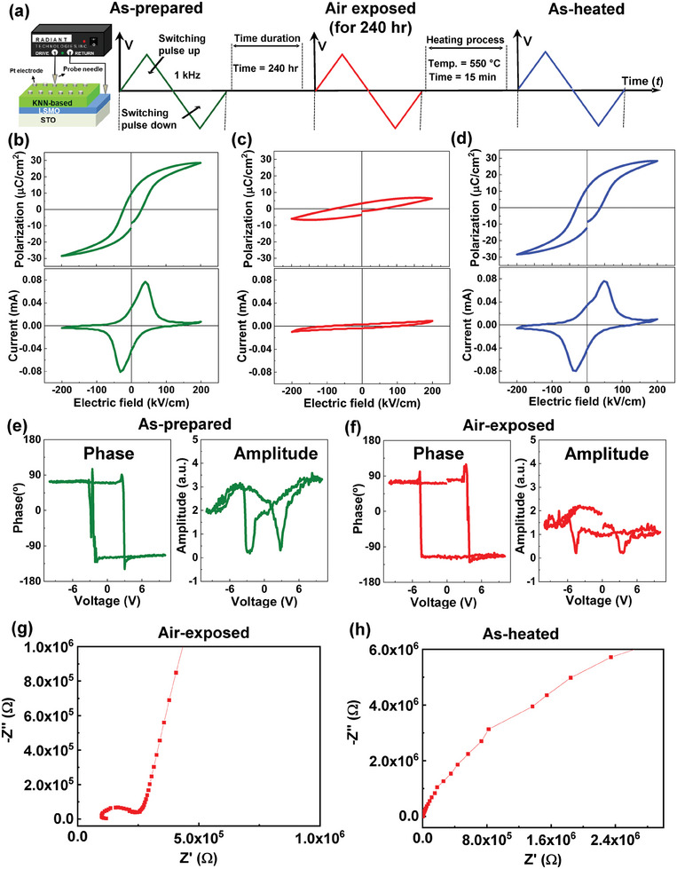
Understanding microscopic mechanisms of polarization retention characteristics in ferroelectric thin films is of great significance for exploring unusual physical phenomena inaccessible in the bulk counterparts and for realizing thin-film-based functional electronic devices. Perovskite (K,Na)NbO3 is an excellent class of lead-free ferroelectric oxides attracting tremendous interest thanks to its potential applications to nonvolatile memory and eco-friendly energy harvester/storage. Nonetheless, in-depth investigation of ferroelectric properties of (K,Na)NbO3 films and the following developments of nano-devices are limited due to challenging thin-film fabrication associated with nonstoichiometry by volatile K and Na atoms. Herein, ferroelectric (K,Na)NbO3 films of which the atomic-level geometrical structures strongly depend on thickness-dependent strain relaxation are epitaxially grown. Nanopillar crystal structures are identified in fully relaxed (K,Na)NbO3 films to the bulk states representing a continuous reduction of switchable polarization under air environments, that is, polarization retention failures. Protonation by water dissociation is responsible for the humidity-induced retention loss in nano-columnar (K,Na)NbO3 films. The protonation-driven polarization retention failure originates from domain wall pinning by the accumulation of mobile hydrogen ions at charged domain walls for effective screening of polarization-bound charges. Conceptually, the results will be utilized for rational design to advanced energy materials such as photo-catalysts enabling ferroelectric tuning of water splitting.

Keywords: (K,Na)NbO3; epitaxy; ferroelectric; polarization retention loss; thin film.


Conflict of interest statement

The authors declare no conflict of interest.

Figures

Figure 1
Figure 1
Epitaxial KNN/LSMO thin film heterostructures grown on SrTiO3 (001) substrates. a) Schematic 2D diagram of the 600 nm‐thick KNN/LSMO heterostructure films on SrTiO3 (001) substrates. Note that the bulk pseudocubic (pc) lattice constants of the KNN single crystal are a pc = 3.976, b pc = 3.932, and c pc = 3.969 Å.[ 40 ] b) The XRD analyses of the as‐grown KNN (≈600 nm)/LSMO (≈35 nm) hetero‐bilayer thin films. From the rocking‐curve measurement of the thicker KNN (002) Bragg peak in the inset of Figure 1b, we identified that the FWHM was ≈0.48°, nearly twice (≈0.30°) to 600 nm‐thick KNN/LSMO (≈15 nm) thin films epitaxially grown on SrTiO3 (001) substrates (inset in the Figure S2, Supporting Information). c) The AFM topography image of the KNN (≈600 nm)/LSMO (≈35 nm) films on SrTiO3 substrates. d) High‐resolution RSMs of pure KNN (≈600 nm)/LSMO (≈35 nm) films around the (103) Bragg peaks of SrTiO3 (001) substrates. e) The cross‐sectional STEM image of the as‐grown KNN (≈600 nm)/LSMO (≈35 nm) films on the SrTiO3 substrates where the f) nano‐columnar KNN film is shown in the enlarged view. The scale bar in the STEM image is 500 nm.
Figure 2
Figure 2
a) The cross‐sectional STEM image of the as‐grown KNN (≈600 nm)/LSMO (≈35 nm) films on the STO substrates with a clear nanopillar geometry. The scale bar in the STEM image is 200 nm. b) The O‐K edge of the EELS spectra (i.e., the peak “c”) between regions 1 and 2 of the nano‐columnar KNN films. In the shaded rectangular region marked by the peak “c” near the electron energy loss of 545 eV, the 2 peaks highlighted by 2 red arrows in the red spectrum are associated with region 1 whereas a single peak highlighted by a blue arrow was linked to spectra of region 2. The reference spectra of NbO and Nb2O5 spectra are shown in black and green colors, respectively.[ 45 ]
Figure 3
Figure 3
Extracted maximum (P max+ and P max−) and remnant (P rem+ and P rem−) polarization values of the epitaxial KNN (≈600 nm)/LSMO (≈35 nm) hetero‐bilayer thin films on SrTiO3 substrates with varying time (i.e., the polarization values of the KNN films were obtained up to 240 h). The polarization values of the as‐prepared, air exposure for 120 h and air exposure of 240 h were highlighted with green, orange, and red rectangles, respectively in Figure 3a. The polarization‐electric field (PE) hysteresis loops and the corresponding switching current (IE) loops of the KNN (≈600 nm)/LSMO (≈35 nm) hetero‐bilayer thin films in the b) as‐grown state (green color), c) at 120 h (orange color), and d) 240 h (red color).
Figure 4
Figure 4
Electrical resistance and leakage current density experiments of the 600 nm‐thick KNN films. a) Schematic diagram and the optical photograph of an electrical resistance experiment for the 600 nm‐thick KNN sample. b) Resistive responses of 600 nm‐thick KNN (≈600 nm) films, a stepwise decrease in the electrical resistance of KNN sensors was observed in the air‐exposed KNN (≈600 nm) films. c–e) Leakage current results of the KNN (≈600 nm) films. (c) Schematic diagram of the leakage current obtained at the applied voltage of 3 and −3 V. At room temperature, the poling voltage was first set to 15 V and then −15 V, the step size of the increasing voltage was 0.1 V. The leakage current density data of the KNN (≈600 nm) films were acquired both in the (d) air‐exposed and (e) as‐heated state.
Figure 5
Figure 5
X‐ray photoelectron spectroscopy (XPS) spectra at the O 1s of the KNN (≈600 nm) grown on SrTiO3 substrates for a) air‐exposed and b) as‐heated. The time‐of‐flight secondary ion mass spectrometry (TOF‐SIMS) measurements. c, d) The TOF‐SIMS 3D rendering maps of H+ signals and the corresponding in‐depth scanning signal in the air‐exposed (for 240 h) epitaxial KNN (≈600 nm)/LSMO (≈35 nm) hetero‐bilayer thin films. The amplitude of the scanning signals from 0 to 100 sputter time (s) in the air‐exposed and as‐heated case were highlighted by the red and green rectangles, respectively. After thermal heat treatment, the amplitude of the scanning signal reduced 3 times the KNN film in the air‐exposed state.
Figure 6
Figure 6
a) The graphical illustration of the epitaxial KNN (≈600 nm)/LSMO (≈35 nm) hetero‐bilayer thin films for the PE hysteresis and IE loops measurements in the as‐prepared (green), air‐exposed (red), and as‐heated (blue) states. b–d) The PE hysteresis loops and the corresponding IE loops of the KNN (≈600 nm)/LSMO (≈35 nm) hetero‐bilayer thin films in each step of as‐prepared, air‐exposed, and as‐heated states. The PFM phase and amplitude signals of the KNN (≈600 nm)/LSMO (≈35 nm) hetero‐bilayer thin films in the e) as‐prepared and f) air‐exposed states. The butterfly‐shaped PFM amplitude responses were reduced in the air‐exposed KNN sample compared with that in the as‐prepared sample showing that the polarization response was suppressed in the air‐exposed sample. Impedance spectroscopy of the g) air‐exposed and the h) as‐heated KNN (≈600 nm) films.

References

    1. Fatuzzo E., Merz W. J., Ferroelectricity, North‐Holland Pub. Co., Amsterdam 1967.
    1. Scott J. F., Araujo C. A. P. d., Science 1989, 246, 1400. - PubMed
    1. Scott J. F., Science 2007, 315, 954. - PubMed
    1. Khan A. I., Keshavarzi A., Datta S., Nat. Electron. 2020, 3, 588.
    1. Chen P., Zhong X., Zorn J. A., Li M., Sun Y., Abid A. Y., Ren C., Li Y., Li X., Ma X., Chen L.‐Q., Pan X., Nat. Commun. 2020, 11, 1840. - PMC - PubMed

LinkOut - more resources