

Quantum sensing with optically accessible spin defects in van der Waals layered materials
- PMID: 39496613
- PMCID: PMC11535532
- DOI: 10.1038/s41377-024-01630-y
Quantum sensing with optically accessible spin defects in van der Waals layered materials
Abstract
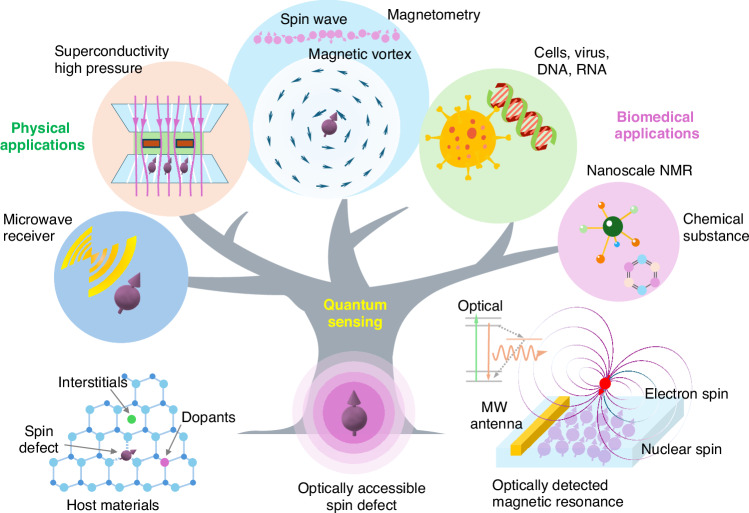
Quantum sensing has emerged as a powerful technique to detect and measure physical and chemical parameters with exceptional precision. One of the methods is to use optically active spin defects within solid-state materials. These defects act as sensors and have made significant progress in recent years, particularly in the realm of two-dimensional (2D) spin defects. In this article, we focus on the latest trends in quantum sensing that use spin defects in van der Waals (vdW) materials. We discuss the benefits of combining optically addressable spin defects with 2D vdW materials while highlighting the challenges and opportunities to use these defects. To make quantum sensing practical and applicable, the article identifies some areas worth further exploration. These include identifying spin defects with properties suitable for quantum sensing, generating quantum defects on demand with control of their spatial localization, understanding the impact of layer thickness and interface on quantum sensing, and integrating spin defects with photonic structures for new functionalities and higher emission rates. The article explores the potential applications of quantum sensing in several fields, such as superconductivity, ferromagnetism, 2D nanoelectronics, and biology. For instance, combining nanoscale microfluidic technology with nanopore and quantum sensing may lead to a new platform for DNA sequencing. As materials technology continues to evolve, and with the advancement of defect engineering techniques, 2D spin defects are expected to play a vital role in quantum sensing.
© 2024. The Author(s).
Conflict of interest statement
The authors declare no competing interests.
Figures


References
-
- Alsid, S. T. et al. Solid-state microwave magnetometer with picotesla-level sensitivity. Phys. Rev. Appl.19, 054095 (2023).
-
- Liu, G. Q., Liu, R. B. & Li, Q. Nanothermometry with enhanced sensitivity and enlarged working range using diamond sensors. Acc. Chem. Res.56, 95–105 (2023). - PubMed
Grants and funding
LinkOut - more resources
Full Text Sources
Research Materials
