. 2024 Nov 6;3(1):160.
doi: 10.1038/s44172-024-00308-y.

Kinetic inductance current sensor for visible to near-infrared wavelength transition-edge sensor readout

Affiliations

Kinetic inductance current sensor for visible to near-infrared wavelength transition-edge sensor readout

Paul Szypryt et al. Commun Eng. .

Abstract

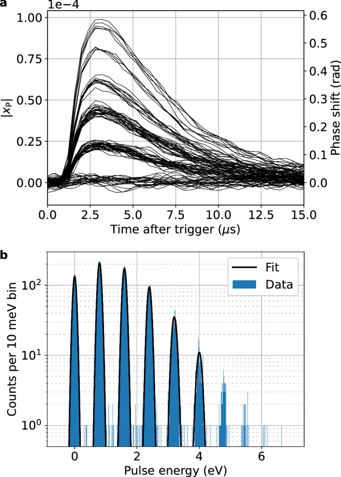
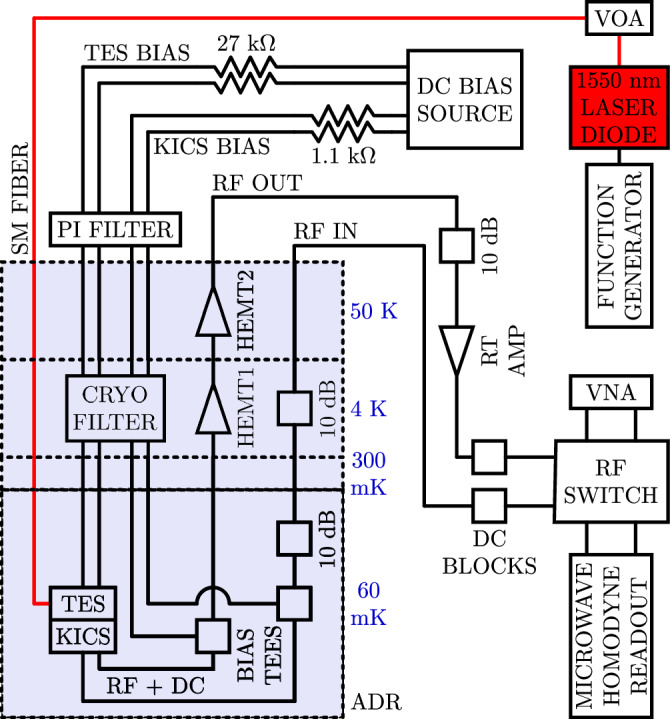
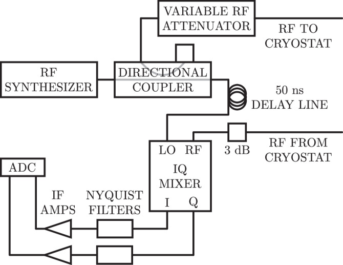
Single-photon detectors based on the superconducting transition-edge sensor are used in a number of visible to near-infrared applications, particularly for photon-number-resolving measurements in quantum information science. To be practical for large-scale spectroscopic imaging or photonic quantum computing applications, the size of visible to near-infrared transition-edge sensor arrays and their associated readouts must be increased from a few pixels to many thousands. In this manuscript, we introduce the kinetic inductance current sensor, a scalable readout technology that exploits the nonlinear kinetic inductance in a superconducting resonator to make sensitive current measurements. Kinetic inductance current sensors can replace superconducting quantum interference devices for many applications because of their ability to measure fast, high slew-rate signals, their compatibility with standard microwave frequency-division multiplexing techniques, and their relatively simple fabrication. Here, we demonstrate the readout of a visible to near-infrared transition-edge sensor using a kinetic inductance current sensor with 3.7 MHz of bandwidth. We measure a readout noise of 1.4 pA / Hz , considerably below the detector noise at frequencies of interest, and an energy resolution of (0.137 ± 0.001) eV at 0.8 eV, comparable to resolutions observed with non-multiplexed superconducting quantum interference device readouts.


Conflict of interest statement

The authors declare no competing interests.

Figures

Fig. 1
Fig. 1. Schematic and micrograph of a NbTiN kinetic inductance current sensor (KICS) implementation.
A 20 nm thick NbTiN layer is used to form an interdigitated capacitor, C, and a 0.7 μm wide inductor, LKI, that varies nonlinearly with input current. The resonator is inductively coupled to a microstrip transmission line through a set of meandering structures with combined inductance LC. A set of bias tees is used to insert DC current into the nonlinear inductor, and a superconducting switch, SWS, is used to trap this bias current in the device and form a persistent current, IP. In this implementation, SWS is realized with Al wire bonds closing a gap in the microstrip transmission line, as represented by the blue ovals drawn over the micrograph in (b). Near the bottom of the schematic, inductor LLP and resistor RLP form a low-pass filter that separates the microwave circuit of the resonator from that of the lower frequency device (e.g., detector) being read out. Similar to LC, the inductance LLP is formed through a set of inductive meanders, here connecting the resonator to bond pads. The components inside the dashed boxes in (a) are not part of the NbTiN KICS chip and are therefore not pictured in (b). Instead, the bias tees are assembled onto the device box and RLP is wire bonded into the circuit.
Fig. 2
Fig. 2. Full kinetic inductance current sensor (KICS) and transition-edge sensor (TES) assembly.
a Shows a photograph of the full device assembly. Here, a visible to near-infrared TES is mounted inside a zirconia (ZrO2) sleeve that is used to align the TES to an optical fiber. Also pictured is the KICS chip and resistors that form the readout circuit. b Shows the full device circuit when set up for photon detection. The TES with variable resistance, RTES, is biased using a shunt resistor, Rsh. The TES current, ITES, is coupled to a KICS with persistent current IP.
Fig. 3
Fig. 3. Kinetic inductance current sensor (KICS) responsivity.
a Shows the device transmission magnitude, ∣S21∣, as DC current, IDC, is swept, with the resonance moving from higher to lower frequencies. The dip in ∣S21∣ at high frequencies is due to parasitic capacitance to ground, but this is largely inconsequential for this measurement as increasing IDC to the operating point moves the KICS resonance sufficiently far from the parasitic resonance. b Shows the resonator fractional frequency shift magnitude, ∣x∣, as a function of IDC. The responsivity, dx∣/dI, was measured to be 0.25 mA−1 at a bias current of 1.95 mA (local slope). This bias point is indicated in both panels with the vertical dashed line.
Fig. 4
Fig. 4. Transition-edge sensor (TES) current-voltage (IV) characteristic curves.
The TES voltage, VTES, was swept at temperatures between 60 mK and 190 mK, and the current, ITES, was read out through the kinetic inductance current sensor. The inset shows the IV curve at 60 mK, which is the control temperature used for subsequent measurements.
Fig. 5
Fig. 5. Noise power spectral density (PSD).
The complex transmission data were projected onto the frequency and dissipation quadratures, and Fourier transform techniques were used to generate a noise PSD in each quadrature. The measured responsivity was used to convert the noise PSD in fractional frequency shift units, SxP, to a current sensitivity, SI. For visual clarity, the frequency resolution was dynamically adjusted from 1 Hz to 1 kHz between the low and high frequency regions. The frequency-quadrature noise was also measured in a separate cooldown with the TES disconnected from the circuit, reflecting the Johnson noise contribution from the filter.
Fig. 6
Fig. 6. Response to 1550 nm photons.
a Shows the fractional frequency shift response, ∣xP∣, to the first 100 1550 nm photon pulses, with clear separation by photon number. A total of 10,000 traces were filtered and energy calibrated to produce the spectrum in (b). The peaks in the spectrum were fit to Gaussian distributions with the extracted width representing the energy resolution, ΔE, at that peak energy (see Table 1).
Fig. 7
Fig. 7. Experimental setup schematic.
The setup is separated into optical, DC, and RF circuits. The optical circuit is used to source single photons to the TES detector through a single-mode (SM) fiber, and photon pulses are shaped using a function generator and variable optical attenuator (VOA). The DC circuit is used to bias the transition-edge sensor (TES) and kinetic inductance current sensor (KICS). Characterization measurements are done with the RF circuit through a vector network analyzer (VNA) and microwave homodyne readout. The RF signals are amplified using a set of cryogenic high-electron mobility transistor (HEMT) amplifiers and a room temperature amplifier (RT amp). The shaded region represents the interior of the adiabatic demagnetization refrigerator (ADR), separated by temperature stage.
Fig. 8
Fig. 8. Microwave homodyne readout schematic.
Central to the readout is an IQ (in-phase and quadrature) mixer, which transforms the microwave frequency response of the kinetic inductance current sensor (KICS) into baseband I and Q signals through mixing with a reference signal at the local oscillator (LO) port. These I and Q signals are Nyquist filtered and amplified with intermediate frequency amplifiers (IF amps) before being digitized by an analog-to-digital converter (ADC). The digitized I and Q outputs are used to characterize the device noise and photon response.

References

    1. Andrews, D. H., Brucksch, W. F., Ziegler, W. T. & Blanchard, E. R. Attenuated superconductors I. For measuring infra-red radiation. Rev. Sci. Instrum.13, 281–292 (1942).
    1. Irwin, K. D. & Hilton, G. C. in Transition-Edge Sensors,Cryogenic Particle Detection, of Topics in Applied Physics (ed. Enss, C.) Vol. 99 (Springer, 2005).
    1. Richards, P. L. Bolometers for infrared and millimeter waves. J. Appl. Phys.76, 1–24 (1994).
    1. Gildemeister, J. M., Lee, A. T. & Richards, P. L. A fully lithographed voltage-biased superconducting spiderweb bolometer. Appl. Phys. Lett.74, 868–870 (1999).
    1. Irwin, K. D., Hilton, G. C., Wollman, D. A. & Martinis, J. M. X-ray detection using a superconducting transition-edge sensor microcalorimeter with electrothermal feedback. Appl. Phys. Lett.69, 1945–1947 (1996).

LinkOut - more resources