. 2024 Nov 18;14(1):28448.
doi: 10.1038/s41598-024-79881-3.

High-voltage FinFET with floating poly and high-k material for enhanced intrinsic gain and safe operating area

Affiliations

High-voltage FinFET with floating poly and high-k material for enhanced intrinsic gain and safe operating area

Kyounghwan Oh et al. Sci Rep. .

Abstract

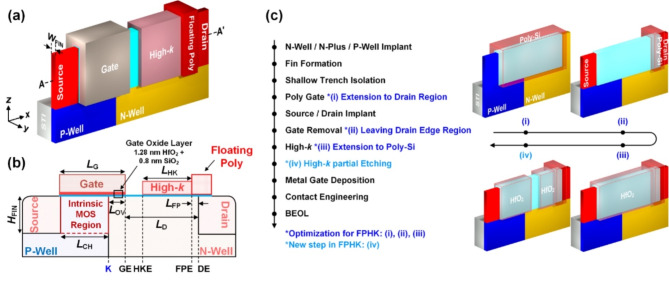
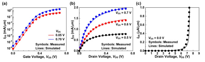
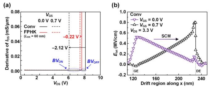
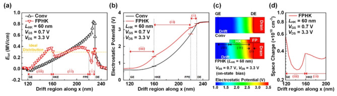
We propose a new drain-extended FinFET (DeFinFET) that can improve the intrinsic gain (gm/gds) and the electrical safe operating area (SOA). This structure features a novel utilization of the drain potential by using a floating poly (FP) and split high-k material (HK) on the drain and drift regions. This method effectively controls the potential drop profile within the drift region, which makes a uniform electric field distribution in the gate-on state. The evenly distributed electric field significantly increases the on-state breakdown voltage (7.33 V) compared to a conventional structure (5.89 V). In addition, it prevents the device from operating in an undesirable quasi-saturation mode, even after space charge modulation. This operation distinguishes our results from other studies, showing a notable improvement in gm/gds. Moreover, electron accumulation is induced in the drift region, leading to a significant decrease in the on-resistance. As a result, the proposed device demonstrates clear advantages in high-voltage applications with a 45% expanded electrical SOA over conventional DeFinFET.


Conflict of interest statement

Declarations Competing interests The authors declare no competing interests.

Figures

Fig. 1
Fig. 1
Proposed structure (FPHK) utilized in this study. (a) Bird’s eye view and (b) A-A’ cross-sectional view. Floating poly (FP) is partially introduced on the N-Well and drain junction, and high-k material (HK) is selectively deposited on the drift region adjacent to FP. The potential of FP is transmitted to the drift region through HK, leading to a potential modulation within the drift region. (c) Process flow for FPHK. The black text outlines the conventional Drain-extended FinFET. (i)-(iii) steps depict optimization factors for FPHK, and (iv) step describes an additional step specific to FPHK. Specific sections of the spacers and oxide are deliberately left out to improve the visual clarity of the structure.
Fig. 2
Fig. 2
Calibration results for measured data. (a) Transfer curve at VDS = 0.05 and 0.7 V. (b) Output curve at VGS = 0.5, 0.6, and 0.7 V. (c) Breakdown characteristic curve at VGS = 0.0 V. The simulation framework is fine-tuned to accurately capture the performance of nano-scale FinFET and breakdown mechanism in DeFinFET.
Fig. 3
Fig. 3
(a) Derivative of IDS as a function of VDS with VGS of 0.0 V and 0.7 V for Conv and FPHK. The breakdown points representing BVON and BVOFF are indicated. (b)Elat under the gate-off and on state at VDS = 3.3 V for Conv. There is no significant difference between BVOFF and BVON for FPHK, while for Conv, the electric field is concentrated at the DE region upon gate-on, leading to a significant decrease in BVON.
Fig. 4
Fig. 4
(a)Elat and (b) electrostatic potential in the drift region along the horizontal cut-line, and (c) electrostatic potential captured in the drift region under the on-state bias condition for Conv and FPHK. Conv shows a high electric peak at DE, whereas FPHK demonstrates an evenly distributed Elat with the suppression of sharp potential drop in the drift region. (d) Space charge for FPHK along the horizontal cut-line under the on-state bias condition at the regions (ii) and (iii).
Fig. 5
Fig. 5
(a)BVON and RON for Conv and FPHK with different LHK. Throughout the entire LHK range, FPHK shows increased BVON and reduced RON compared to Conv. (b)Elat and (c)Elat, max for different LHK under the on-state bias condition for Conv and FPHK. At LHK = 60 nm, FPHK achieves the lowest Elat, max, showing a balance between electric field distribution within the region (ii) and (iii). (d) Electron density for Conv and FPHK under the RON extraction bias condition. The potential of FP, increased by drain bias, is transmitted to the drift region through HK, resulting in electron accumulation within the drift region.
Fig. 6
Fig. 6
(a) Transfer and (b) output curves for Conv and FPHK. (c)gm, (d)gds, and (e)VK for Conv and FPHK as a function of IDS. FPHK shows an improved gm flatness compared to Conv. As IDS increases, Conv shows a sharp increase in gds after SCM, while the increase in FPHK is suppressed. (f) Electron Density along the horizontal cut-line under the on-state bias condition for Conv and FPHK. FPHK shows a clearer pinch-off.
Fig. 7
Fig. 7
(a)gm/gds for Conv and FPHK as a function of IDS. After SCM, Conv shows a sharp decrease in gm/gds, while FPHK demonstrates an improved flatness with a significantly reduced decrease rate. (b) Electrical SOA for Conv and FPHK. FPHK shows a 45% expanded electrical SOA compared to Conv.

References

    1. Song, T. et al. A 14nm FinFET 128 Mb 6T SRAM with VMIN-enhancement techniques for low-power applications. In IEEE Int. Solid-State Circuits Conf. Dig. Tech. Papers (ISSCC) 232–233 (2014).
    1. Yeh, C. C. et al. A low operating power FinFET transistor module featuring scaled gate stack and strain engineering for 32/28nm SoC technology. In International Electron Devices Meeting (IEDM) 34.1.1–34.1.4 (2010).
    1. Kumar, B. S., Paul, M., Gossner, H. & Shrivastava, M. Physical insights into the ESD Behavior of Drain Extended FinFETs (DeFinFETs) and Unique Current Filament dynamics. IEEE Trans. Electron. Devices. 67 (7), 2717–2724 (2020).
    1. Paul, M. et al. Drain-extended FinFET with embedded SCR (DeFinFET-SCR) for high-voltage ESD Protection and Self-protected designs. IEEE Trans. Electron. Devices. 66 (12), 5072–5079 (2019).
    1. Kumar, B. S., Paul, M. & Shrivastava, M. On the design challenges of drain extended FinFETs for advance SoC integration. In Int. Conf. Simul. Semicond. Processes Devices (SISPAD) 189–192 (2017).

LinkOut - more resources