

Repetitive ultramicrotome trimming and SEM imaging for characterizing printed multilayer structures
- PMID: 39567618
- PMCID: PMC11579308
- DOI: 10.1038/s41598-024-79717-0
Repetitive ultramicrotome trimming and SEM imaging for characterizing printed multilayer structures
Abstract
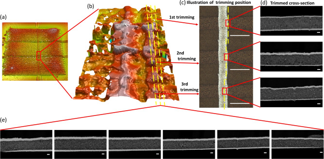
Ultramicrotomy is a well-established technique that has been applied in biology and medical research to produce thin sections or a blockface of an embedded sample for microscopy. Recently, this technique has also been applied in materials science or micro- and nanotechnology as a sample preparation method for subsequent characterization. In this work, an application of ultramicrotomy for the cross-section preparation of an inkjet-printed multilayer structure is demonstrated. The investigated device is a capacitor consisting of three layers. The top and bottom electrodes are printed with silver nanoparticle ink and the dielectric layer with a ceramic nanoparticle/polymer ink. A 3D profilometer is initially used to study the surface morphology of the printed multilayer. The measurements show that both electrodes exhibit a coffee-ring effect, which results in an inhomogeneous layer structure of the device. To obtain precise 3D information on the multilayer, cross-sections must be prepared. Argon ion beam milling is the current gold standard to produce a single cross-section in good quality, however, the cross-section position within the multilayer volume is poorly defined. Moreover, the milling process requires a significant investment of time and resources. Herein, we develop an efficient method to realize repetitive cross-section preparation at well-defined positions in the multilayer volume. Repetitive cross-sections are exposed by trimming with an ultramicrotome (UM) and this blockface is subsequently transferred into a scanning electron microscope (SEM) for imaging. A combination of custom-modified UM and SEM specimen holders allows repeated transfer of the clamped multilayer sample between instruments without damage and with high positioning accuracy. This novel approach enhances the combination of an established ultramicrotome and a SEM for multilayer sample volume investigation. Thus, a comprehensive understanding of printed multilayer structures can be gained, to derive insights for optimization of device architecture and printing process.
Keywords: Inkjet printing; Multilayer; SEM imaging; Ultramicrotomy.
© 2024. The Author(s).
Conflict of interest statement
Declarations. Competing interests: The authors declare no competing interests.
Figures


Similar articles
-
Fabrication of Flexible Multilayer Composite Capacitors Using Inkjet Printing.Nanomaterials (Basel). 2020 Nov 20;10(11):2302. doi: 10.3390/nano10112302. Nanomaterials (Basel). 2020. PMID: 33233838 Free PMC article.
-
Geometry Control of Source/Drain Electrodes in Organic Field-Effect Transistors by Electrohydrodynamic Inkjet Printing.Materials (Basel). 2020 Nov 5;13(21):4974. doi: 10.3390/ma13214974. Materials (Basel). 2020. PMID: 33167331 Free PMC article.
-
Polymerizable Ceramic Ink System for Thin Inkjet-Printed Dielectric Layers.ACS Appl Mater Interfaces. 2020 Jan 15;12(2):2974-2982. doi: 10.1021/acsami.9b18610. Epub 2020 Jan 2. ACS Appl Mater Interfaces. 2020. PMID: 31845575
-
Applications of scanning electron microscopy and focused ion beam milling in dental research.Eur J Oral Sci. 2022 Apr;130(2):e12853. doi: 10.1111/eos.12853. Epub 2022 Mar 14. Eur J Oral Sci. 2022. PMID: 35288994 Review.
-
Nanoskiving: a new method to produce arrays of nanostructures.Acc Chem Res. 2008 Dec;41(12):1566-77. doi: 10.1021/ar700194y. Acc Chem Res. 2008. PMID: 18646870 Review.
References
-
- Rowenhorst, D. J., Nguyen, L., Murphy-Leonard, A. D. & Fonda, R. W. Characterization of microstructure in additively manufactured 316L using automated serial sectioning. Curr. Opinion Solid State Mater. Sci.24, 100819 (2020).
-
- Torrance, R. & James, D. The state-of-the-art in ic reverse engineering. in International Workshop on Cryptographic Hardware and Embedded Systems, 363–381 (Springer, 2009).
-
- Li, Y. & Goyal, D. Fault isolation and failure analysis of 3D packaging. 3D Microelectronic Packaging: From Architectures to Applications 575–617 (2021).
-
- Hayat, M. A. et al.Principles and Techniques of Electron Microscopy: Biological Applications, 4th Edn. (Cambridge University Press, 2000).
LinkOut - more resources
Full Text Sources
