. 2024 Nov 20;29(22):5480.
doi: 10.3390/molecules29225480.

Structure, Optical and Electrical Properties of Nb(Zn) Doped Sol-Gel ITO Films: Effect of Substrates and Dopants

Affiliations

Structure, Optical and Electrical Properties of Nb(Zn) Doped Sol-Gel ITO Films: Effect of Substrates and Dopants

Mariuca Gartner et al. Molecules. .

Abstract

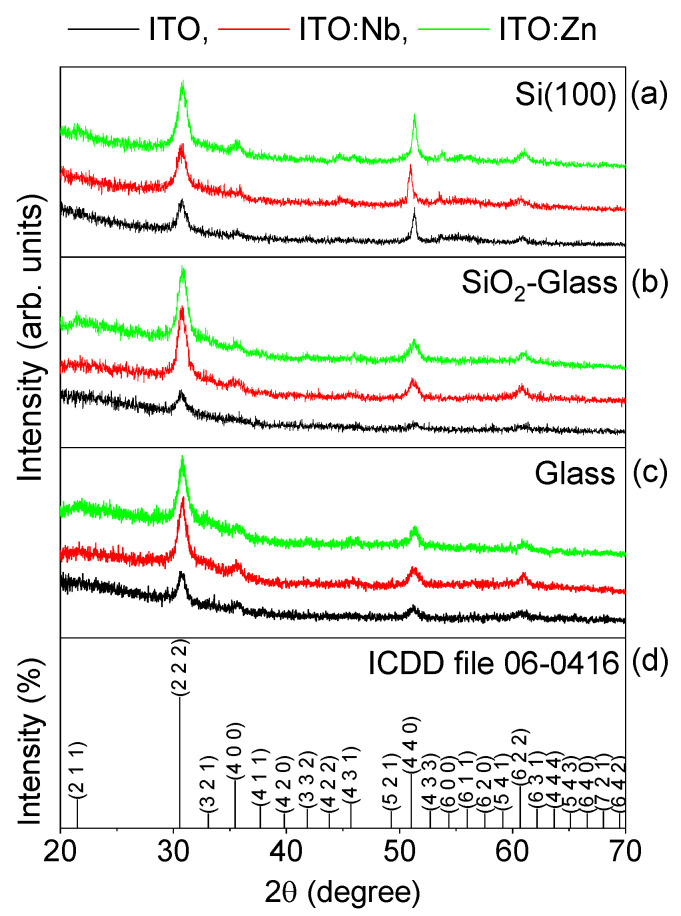
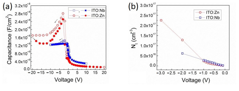
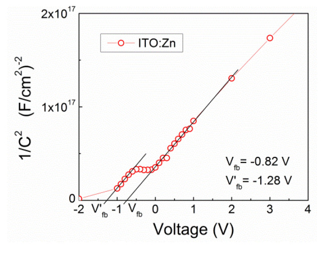
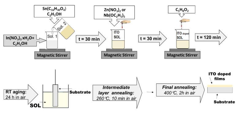
We present comparative studies of sol-gel ITO multilayered films undoped and doped with Nb or Zn (4 at.%). The films were obtained by successive depositions of five layers using the dip-coating sol-gel method on microscopic glass, SiO2/glass, and Si substrates. The influence of the type of substrates and dopant atoms on the structure and optical properties of the sol-gel ITO thin films is examined and discussed in detail. XRD patterns of these layers showed a polycrystalline structure with an average crystallite size of <11 nm. Raman spectroscopy confirmed the chemical bonding of dopants with oxygen and showed the absence of crystallized Nb(Zn)-oxide particles, indicated by the XRD pattern. Spectroscopic Ellipsometry and AFM imaging revealed a clear dependence of the optical parameters and surface morphology of the ITO and ITO:Nb(Zn) thin films on the type of substrates and dopants. The analysis of the current-voltage and capacitance-voltage characteristics of the Al/ITO/Si structures revealed the presence of charge carrier traps in the ITO bulk and the ITO-Si interface. The densities of these traps are obtained and the character of the current transport mechanism is established.

Keywords: Nb(Zn) doped ITO thin films; electrical properties; microstructure; optical properties; sol–gel films.


Conflict of interest statement

The authors declare no conflicts of interest.

Figures

Figure 1
Figure 1
XRD patterns of the undoped (black line), Nb- (red line), and Zn-doped ITO (green line) thin films, deposited on Si(100) (a), SiO2/glass (b), glass (c) substrates. The ICDD file no. 6-0416 is given as a reference in (d).
Figure 2
Figure 2
The deconvolution of the main (222) reflections into Gaussian profiles as a function of the substrate type. The diffractograms are corrected with the baselines.
Figure 3
Figure 3
2D AFM images of bare substrates/undoped ITO (ac), Zn-doped/Nb-doped ITO films (df); superimposed characteristic line-scans of the undoped and Zn(Nb) doped ITO films on glass (g), SiO2/glass (h) and Si (i) substrates. The line-scans were collected at the positions indicated in the AFM figures by horizontal red lines; random surface particles are marked along the lines between two red small arrows.
Figure 4
Figure 4
RMS roughness of undoped and Zn(Nb) doped ITO films in comparison to the RMS values of the bare substrates.
Figure 5
Figure 5
SEM micrographs at different magnifications: ×100,000 (a), ×400,000 (b), and EDX spectrum (c) of ITO:Nb film on Si substrate.
Figure 6
Figure 6
Raman spectra of sol–gel films on Si substrate: ITO (a—black), ITO:Nb (b—red), and ITO:Zn (c—green).
Figure 7
Figure 7
Refractive index (n), optical band gap (Eg) (a); and film thickness (tox), porosity (P) (b); obtained from the SE data analysis, for undoped and doped ITO thin films on different substrates.
Figure 8
Figure 8
Optical transmittance of undoped and doped ITO films deposited on glass and SiO2/glass substrates, respectively.
Figure 9
Figure 9
Electrical parameters: specific resistivity (ρ) (a), mobility (µ) (b), carrier concentration (N) (c), and conductivity (σ) (d), obtained by SE analysis for undoped and Nb(Zn) doped ITO films deposited on glass, SiO2/glass, and Si substrates; compared with those obtained by Hall measurements from [3,22].
Figure 10
Figure 10
I-V characteristics of Al/ITO/Si structures with undoped (triangles) and Nb (squares) and Zn (circles) doped sol–gel ITO films. In the insert, the hysteresis effect is illustrated for the undoped and Nb-doped ITO films.
Figure 11
Figure 11
Specific resistivity (ρ) versus electric field applied to the Al/ITO/Si structures with undoped ITO (triangles) and Nb (squares) or Zn (circles) doped ITO multilayers.
Figure 12
Figure 12
Logarithm of room-temperature forward current density as a function of logarithm absolute voltage for the Al/ITO/Si structures with undoped ITO (triangles) and Nb (squares) or Zn (circles) doped ITO films.
Figure 13
Figure 13
1 MHz C-V characteristics of Al/ITO:Nb(Zn)/Si (a) and the density of occupied traps (Nt) in ITO:Nb(Zn) as a function of applied voltage (b).
Figure 14
Figure 14
Mott–Schottky plot represented by Al/ITO:Zn/Si structure.
Figure 15
Figure 15
I-V characteristics of Al/ITO/Si structures with undoped ITO (a) and Nb-doped ITO (b) films, measured at temperatures of 294 K and 77 K.
Figure 16
Figure 16
The flowchart of sol–gel technological procedures for the preparation of undoped and doped ITO thin films.

References

    1. Chen Z., Li W., Li R., Zhang Y., Xu G., Cheng H. Fabrication of Highly Transparent and Conductive Indium–Tin Oxide Thin Films with a High Figure of Merit via Solution Processing. Langmuir. 2013;29:13836–13842. doi: 10.1021/la4033282. - DOI - PubMed
    1. Micali M., Cosentino S., Terrasi A. Structural, Optical and Electrical Characterization of ITO Films Co-Doped with Molybdenum. Sol. Energy Mater. Sol. Cells. 2021;221:110904. doi: 10.1016/j.solmat.2020.110904. - DOI
    1. Gartner M., Anastasescu M., Calderon-Moreno J.M., Nicolescu M., Stroescu H., Hornoiu C., Preda S., Predoana L., Mitrea D., Covei M. Multifunctional Zn-Doped ITO Sol–Gel Films Deposited on Different Substrates: Application as CO2-Sensing Material. Nanomaterials. 2022;12:3244. doi: 10.3390/nano12183244. - DOI - PMC - PubMed
    1. Asare J., Agyei-Tuffour B., Amonoo E.A., Dodoo-Arhin D., Nyankson E., Mensah B., Oyewole O.O., Yaya A., Onwona-Agyeman B. Effects of Substrates on the Performance of Optoelectronic Devices: A Review. Cogent. Eng. 2020;7:1829274. doi: 10.1080/23311916.2020.1829274. - DOI
    1. Lin J., Liang R., Tan H., Peng J., Huang P., Dai J., Li Y., Chen J., Xu H., Xiao P. Optical and Electrical Properties of Niobium-Doped Indium Oxide Thin Films Prepared by Co-Sputtering Technique. Thin Solid Film. 2023;787:140139. doi: 10.1016/j.tsf.2023.140139. - DOI

LinkOut - more resources