. 2023 May 17;12(12):2103-2113.
doi: 10.1515/nanoph-2023-0196. eCollection 2023 Jun.

Multifunctional charge transfer plasmon resonance sensors

Affiliations

Multifunctional charge transfer plasmon resonance sensors

Alemayehu Nana Koya et al. Nanophotonics. .

Abstract

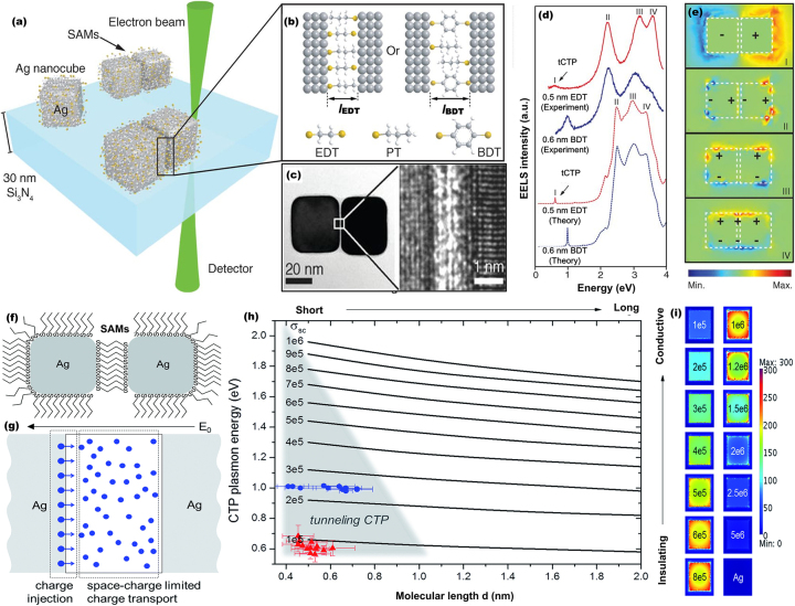
Charge transfer plasmon (CTP) modes arise when metallic nanoparticle dimers are connected by a conductive junction. This offers a unique opportunity to explore electron transport at optical frequencies as well as to attain narrow plasmon resonances that can be broadly modulated from visible to IR regimes, implying their potentials for applications in single-molecule electronics and sensing. This article showcases recent developments in theory and applications of charge transfer plasmon resonances (CTPRs) in various configurations of conductively linked plasmonic nanodimers. In particular, we give a due attention to exploiting ultratunable spectral features of charge transfer plasmon resonances for developing multifunctional plasmonic sensors for bulk, surface, gas and molecular sensing applications. We also discuss the implications of the charge and energy transfer between two plasmonic nanoparticles linked by sub-nanometer thick self-assembled monolayers for single-molecule conductance sensing and molecular electronics. In addition to the well-established plasmonic sensing schemes based on propagating and localized surface plasmon resonances, charge transfer plasmon resonance sensors may open up a new route in efforts to develop multifunctional sensing technologies.

Keywords: charge transfer plasmons; localized surface plasmons; plasmonic sensors; single-molecule conductance sensing.


Figures

Figure 1:
Figure 1:
Illustration of sensing principles based on charge transfer plasmon (CTP) resonances for refractive index sensing (top left), gas sensing (top right), surface sensing (bottom left), and molecular sensing (bottom right). Middle: CTP resonance wavelength shift (Δλ CTP) due to change in the dielectric environment of linked plasmonic nanoparticle dimer.
Figure 2:
Figure 2:
Spectral characteristics of charge transfer plasmon resonances in conductively linked plasmonic (here Au) nanoparticles. (a) Schematic illustration of geometric parameters that define CTP resonances in conductively linked plasmonic nanoparticles. These include nanoparticle size D, junction length L and radius r. (b) Spectral signature of the charge transfer plasmon resonance of connected Au nanoparticles. The CTP mode appears substantially at lower energies compared to other plasmon modes like screened bonding dimer plasmon (SBDP) mode of bridged nanodimer or bonding dimer plasmon (BDP) mode of unbridged nanodimer. Reproduced with permission from [18]. Copyright 2017 AIP Publishing. (c) Tuning CTP resonance of linked Au nanotrimer by changing junction conductance through its geometric parameter (here radius of cylindrical linker). (d) CTP spectral shift of conductively linked Au trimers as a function of junction radius for different nanoparticle shapes. Reproduced with permission from [12] Copyright 2016 AIP Publishing.
Figure 3:
Figure 3:
Active control of charge transfer in plasmonic nanodimers linked by molecular junctions. Top: Schematic illustrations of (a) quantum corrected model mimicing electrron tunneling through a molecular linker and (b) Au nanoparticle dimer functionalized with DNA molecules incorporated into a monolayer of PEG-COOH (left) and integrated with Pd nanoparticless (right). Bottom: TEM analysis, spectroscopy and charge density maps of Pd nanoparticles in plasmonic nanodimers with gap width of (c) 2 nm and (d) 18 nm. Reproduced under terms of the CC-BY license from [27]. Copyright 2018, The Authors, published by Nature Publishing Group.
Figure 4:
Figure 4:
Charge transfer plasmon resonance-based bulk and surface sensing. (a) Schematic of capacitively coupled sub-5 nm dimer (dimer) and conductively coupled dimers with center (dimer-c) and bottom (dimer-b) bridges of 40 nm width. Each cubic Au nanodimer has a height of h = 150 nm. Transmission spectra shift as a function of refractive index for (b) dimer, (c) dimer-c, and (d) dimer-b nanostructures. (e) Bulk sensing performance of dimer, dimer-c, and dimer-b structures based on cladding index n cl = 1.3. (f) Transmission spectra and (g) surface sensitivity characteristics of dimer-b as a function of number of carbon chains. Reproduced with permission from [23]. Copyright 2021, Wiley-VCH.
Figure 5:
Figure 5:
Molecular tunnel junction controlled quantum plasmon resonances in plasmonic nanodimers linked by self-assembled monolayers (SAMs). (a) Schematic illustration of the molecular tunnel junctions made of two Ag nanoparticles bridged by SAMs of EDT (1,2-ethanedithiolates) and BDT (1,4-benzenedithiolates). (b) Active control of the distance between two adjacent Ag nanoparticles through the EDT and BDT thickness. (c) A high-resolution TEM image of the Ag–SAM–Ag junction. (d) Measured EELS spectra and quantum-corrected simulations of extinction spectra of Ag–SAM–Ag nanosystem, confirming quantum tunneling directly observed as tunneling charge transfer plasmon (tCTP) peak. (e) Simulated electric near-field distributions for the designated plasmonic modes I to IV. Reproduced with permission from [29]. Copyright 2014, American Association for the Advancement of Science. (f) Schematic diagram of hybrid Ag–SAM–Ag system. (g) Space-charge corrected electromagnetic model to describe the charge transfer plasmon oscillations of the Ag–SAM–Ag junction, where negative driving field (during half cycles) induces charge transfer from left to right. (h) Constructed parameter map to correlate resonant CTP energies (eV), SAM conductivity σ sc (S/m), and SAM molecular lengths d (nm) in the Ag–SAM–Ag system for fixed Ag nanocube dimesnions. (i) Magnitudes of total electric field enhancements at the Ag/SAM interface for various gap conductivities at respective CTP resonant frequencies. Reproduced with permission from [54]. Copyright 2016, Royal Society of Chemistry.
Figure 6:
Figure 6:
Implication of tunneling charge transfer plasmon (tCTP) for single-molecule conductance sensing. (a) Schematic of conductive (BPDT) and nonconductive (BPT) self-assembled monolayers in plasmonic junctions made of Au nanoparticle-on-mirror (NPoM) configuration. (b) Normalized scattered intensity from individual 60 nm gold nanoparticles on BPT and BPDT. (c) Average SERS spectra normalized by the number of molecules, comparing SERS intensities from BPDT and BPT. Reproduced with permission from [57]. Copyright 2014, American Chemical Society. (d) Schematic illustration of mechanically controllable break junction (MCBJ) SERS setup with molecular structures of BDT and dimeric-BDT. Inset: Hypothetical evolution of the microscopic configuration as the conductance G of the monolayers evolves from high conductance to low conductance. (e) SERS spectra collected when the molecular junction was mechanically controlled at the regimes of high conductance (red), low conductance (green), and breakage (grey), respectively. An ordinary Raman spectrum of BDT powder (brown) is displayed for comparison. Reproduced with permission from [59]. Copyright 2018, Royal Society of Chemistry.

Similar articles

References

    1. Koya A. N., Ji B., Hao Z., Lin J. Resonance hybridization and near field properties of strongly coupled plasmonic ring dimer-rod nanosystem. J. Appl. Phys. . 2015;118:113101. doi: 10.1063/1.4930057. - DOI
    1. Koya A. N., Ji B., Hao Z., Lin J. Controlling optical field enhancement of a nanoring dimer for plasmon-based applications. J. Opt. . 2016;18:055007. doi: 10.1088/2040-8978/18/5/055007. - DOI
    1. Koya A. N., Cunha J., Guerrero-Becerra K. A., et al. Plasmomechanical systems: principles and applications. Adv. Funct. Mater. . 2021;31:2103706. doi: 10.1002/adfm.202103706. - DOI
    1. Maccaferri N., Barbillon G., Koya A. N., Lu G., Acuna G. P., Garo-li D. Recent advances in plasmonic nanocavities for single-molecule spectroscopy. Nanoscale Adv. . 2021;3:633–642. doi: 10.1039/d0na00715c. - DOI - PMC - PubMed
    1. Koya A. N., Zhu X., Ohannesian N., et al. Nanoporous metals: from plasmonic properties to applications in enhanced spectroscopy and photocatalysis. ACS Nano . 2021;15:6038–6060. doi: 10.1021/acsnano.0c10945. - DOI - PMC - PubMed

LinkOut - more resources