Review
. 2023 Mar 22;12(9):1643-1710.
doi: 10.1515/nanoph-2022-0797. eCollection 2023 Apr.

Two-dimensional metal halide perovskites and their heterostructures: from synthesis to applications

Affiliations
Review

Two-dimensional metal halide perovskites and their heterostructures: from synthesis to applications

Athanasia Kostopoulou et al. Nanophotonics. .

Abstract

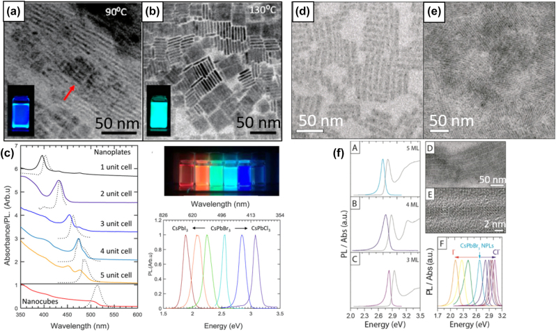
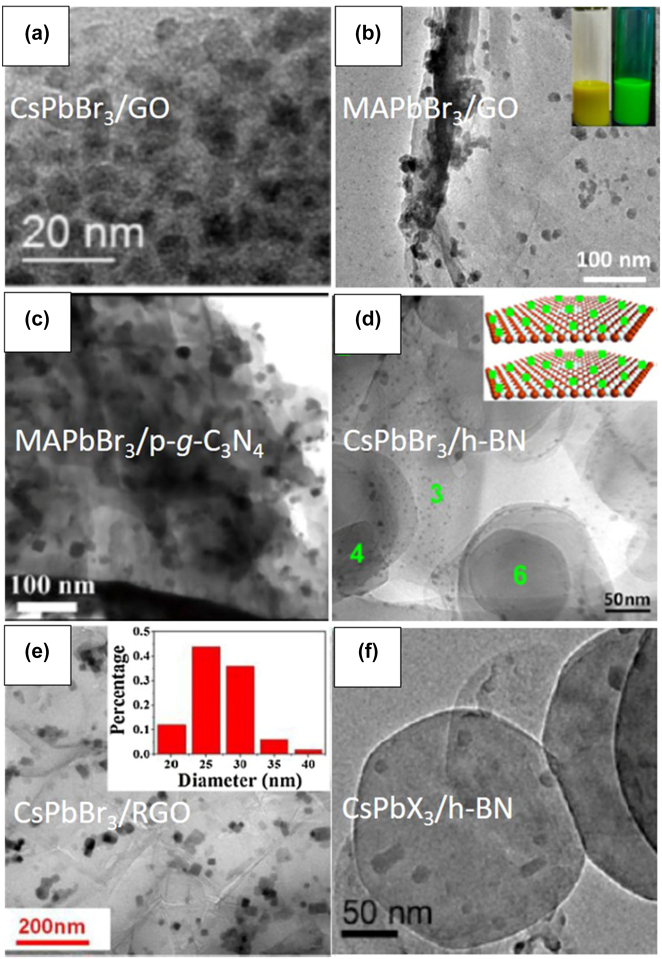
Size- and shape-dependent unique properties of the metal halide perovskite nanocrystals make them promising building blocks for constructing various electronic and optoelectronic devices. These unique properties together with their easy colloidal synthesis render them efficient nanoscale functional components for multiple applications ranging from light emission devices to energy conversion and storage devices. Recently, two-dimensional (2D) metal halide perovskites in the form of nanosheets (NSs) or nanoplatelets (NPls) are being intensively studied due to their promising 2D geometry which is more compatible with the conventional electronic and optoelectronic device structures where film-like components are usually employed. In particular, 2D perovskites exhibit unique thickness-dependent properties due to the strong quantum confinement effect, while enabling the bandgap tuning in a wide spectral range. In this review the synthesis procedures of 2D perovskite nanostructures will be summarized, while the application-related properties together with the corresponding applications will be extensively discussed. In addition, perovskite nanocrystals/2D material heterostructures will be reviewed in detail. Finally, the wide application range of the 2D perovskite-based structures developed to date, including pure perovskites and their heterostructures, will be presented while the improved synergetic properties of the multifunctional materials will be discussed in a comprehensive way.

Keywords: 2D materials; energy conversion; energy storage; perovskite nanocrystals; photodetectors; sensing; synthesis routes.


Figures

Figure 1:
Figure 1:
Schematic illustration of the crystal structure of the metal halide perovskites with chemical formula ABX3 and the formation of the 2D platelets-like morphologies composed of one and six monolayers (a–c). PL spectra and band gap energy for the modification of the bulk structures, to weakly confined nanocubes to strongly confined 2D nanoplatelets/nanosheets (d and e). Adapted with permission from Ref. [1]. Copyright 2021, Wiley.
Figure 2:
Figure 2:
Review content in one scheme. 2D metal halide perovskites, metal halide nanocrystals/2D material heterostructures, enhanced properties, and applications.
Figure 3:
Figure 3:
Photoluminescence (PL) and absorbance spectra of the FAPbI3 NSs, along with indicative transmission electron microscopy (TEM) images (a). ((a) has been reproduced from Ref. [24] with permission from American Chemical Society, copyright 2017). Schematic animation of the HI colloidal synthesis with benzoyl halides (b). Transmission electron microscopy (TEM) photos of the so-formed MAPbCl3 (c), MAPbBr3 (d), and MAPbI3 PNCs (e). Absorbance and photoluminescence (PL) spectra of MAPbCl3 (f), MAPbBr3 (g), and MAPbI3 PNCs (h). ((b)–(h) have been reproduced from Ref. [73] with permission from American Chemical Society, copyright 2018).
Figure 4:
Figure 4:
Schematic representation of the ligand-assisted reprecipitation (LARP) method (a). ((a) has been reproduced from Ref. [28] with permission from American Chemical Society, copyright 2019). Transformation of three-dimensional (3D) cubes into 2D nanostructures in the presence of pyridine (b). ((b) has been reproduced from Ref. [25] with permission from American Chemical Society, copyright 2017). Photograph of typical dispersion solutions of the so-formed FAPbX3 PNCs under UV-light, along with the photoluminescence (PL) spectra that cover a wide range of the visible (c). On the right, energy bandgap variation versus thickness and typical transmission electron microscopy (TEM) photos of the PNCs. ((c) has been reproduced from Ref. [26] with permission from American Chemical Society, copyright 2017). Absorbance and PL of FAPb(Cl1−xBr x )3 PNCs prepared by means of an automated microfluidic platform (d). ((d) has been reproduced from Ref. [27] with permission from American Chemical Society, copyright 2018).
Figure 5:
Figure 5:
First all-inorganic metal halide perovskite NPls synthesized at high temperature (hot-injection method, reaction temperature 90 and 130 °C) (a), (b) and at room temperature (LARP) ((d), (e), low and high concentration samples). Optical properties for NPls of different thicknesses and halide ratio (through anion exchange reactions) (c) and (f). Reprinted with permission from Ref. [11], copyright 2015, American Chemical Society (a)–(c). Reprinted with permission from Ref. [12], copyright 2016, American Chemical Society (d) and (f), https://pubs.acs.org/doi/10.1021/jacs.5b12124 that further permissions related to the material excerpted should be directed to the ACS (d and f).
Figure 6:
Figure 6:
Schematic illustrating the effect of the ligand type on the morphology of the final all-inorganic metal halide perovskite nanocrystals synthesized by LARP method at room temperature (a) and hot injection (b) method. Reprinted with permission from Ref. [92], copyright 2016, American Chemical Society (a). Reprinted with permission from Ref. [94], copyright 2016, American Chemical Society (b).
Figure 7:
Figure 7:
Effect of the metal halides ratio on the NPls morphology in the hot injection approach. Reprinted with permission from Ref. [95], copyright 2018, Wiley.
Figure 8:
Figure 8:
All-inorganic metal halide perovskite NPls synthesized with triple-source ligand assisted reprecipitation method (a). Absorption (purple) and PL spectra (blue) of the CsPbBr3 NPls’ solutions synthesized using metal-oleate precursors with different aging times (b). Proposed mechanism of the NPls formation (c). Reprinted with permission from Ref. [98], copyright 2021, American Chemical Society.
Figure 9:
Figure 9:
NPls synthesized with solvothermal method at 140 (a)–(d) and 100 °C (f)–(i) with different reaction times. Optical absorption and emission spectra for the corresponding samples (e) and (j). (a)–(e) Reprinted with permission from Ref. [103], copyright 2018, The Royal Society of Chemistry. (f)–(j) Reprinted with permission from Ref. [31], copyright 2018, American Chemical Society.
Figure 10:
Figure 10:
Exfoliation and fusion though a ligand-mediated anion exchange (a)–(c) and laser-triggered (d)–(f) process. (a)–(c) Reprinted with permission from Ref. [16], copyright 2020, American Chemical Society. (d)–(f) Reprinted with permission from Ref. [17], copyright 2022, MDPI.
Figure 11:
Figure 11:
All-inorganic metal halide NPls fabricated with external stimuli-triggered processes. NPLs synthesized using a sonication (a)–(f) and microwave reactor (g)–(k). (a)–(f) Reprinted with permission from Ref. [18], copyright 2016, Wiley. (g)–(k) Reprinted with permission from Ref. [104], copyright 2017, Royal Society of Chemistry.
Figure 12:
Figure 12:
Nanosheets’ size control by the reaction time (a)–(d) and the ratio of short to long ligands (e)–(i). (a)–(d) Reprinted with permission from Ref. [110], copyright 2016, Royal Society of Chemistry. (e)–(i) Reprinted with permission from Ref. [21], copyright 2016, American Chemical Society, https://pubs.acs.org/doi/10.1021/jacs.6b03166 and further permissions related to the material excerpted should be directed to the ACS.
Figure 13:
Figure 13:
Metal halide perovskite nanocrystals/2D materials heterostructures fabricated with LARP and hot injection colloidal methods. (a) Reprinted with permission from Ref. [41], copyright 2017, American Chemical Society. (b) Reprinted with permission from Ref. [62], copyright 2019, Elsevier. (c) Reprinted with permission from Ref. [59], copyright 2017, Royal Society of Chemistry. (d) Reprinted with permission from Ref. [50], copyright 2019, American Chemical Society. (e) Reprinted with permission from Ref. [42], copyright 2017, ScienceDirect. (f) Reprinted with permission from Ref. [49], copyright 2019, Royal Society of Chemistry.
Figure 14:
Figure 14:
Metal halide perovskite nanocrystals/2D materials heterostructures synthesized by mixing the nanocrystal solution with the 2D material solutions. (a) Reprinted with permission from Ref. [46], copyright 2018, Wiley. (b) Reprinted with permission from Ref. [47], copyright 2018, Wiley. (c) Reprinted with permission from Ref. [44], copyright 2019, Royal Society of Chemistry. (d) Reprinted with permission from Ref. [52], copyright 2020, American Chemical Society. (e) Reprinted with permission from Ref. [64], copyright 2022, Wiley.
Figure 15:
Figure 15:
Laser-induced Cs4PbBr6/GO heterostructures for different number of irradiation pulses (a)–(g). Proposed conjugation mechanism (h). Reprinted with permission from Ref. [58], copyright 2020, MDPI.
Figure 16:
Figure 16:
CsPbBr3 nanocrystal encapsulated in 2D C3N4 layer fabricated through a solid-state reaction. Fabrication process (a) and TEM images (b). Reprinted with permission from Ref. [54], copyright 2022, Royal Society of Chemistry.
Figure 17:
Figure 17:
Schematic representation of the solvothermal process for the synthesis of 2D CH3NH3PbBr3 NSs (a). CH3NH3PbBr3 NSs optical band gap dependence on number of layers and thickness (b). CH3NH3PbBr3 NSs photodetector characteristics (c). CH3NH3PbBr3 NSs white light emitter in operation and chromaticity coordinates (d). (a)–(d) have been reproduced from Ref. [116] with permission from ACS American Chemical Society, copyright 2020.
Figure 18:
Figure 18:
Schematic animation of the CsPb(Br/Cl)3 perovskite NSs copper doping process (a). Current density and luminance versus voltage characteristics of the developed blue LED device based on copper-dopped and pristine CsPb(Br/Cl)3 NSs (b). (a) and (b) have been reproduced from Ref. [117] with permission from Elsevier, copyright 2022.
Figure 19:
Figure 19:
Schematic representation of the solution process for the synthesis of MAPbBr3 NPls used in the first NPls-based LED device which is also shown schematically and in operation (a). (a) has been reproduced from Ref. [118] with permission from Wiley Online Library, copyright 2016). Indicative transmission electron microscopy (TEM) profiles of CH3NH3PbBr3 crystals with layers n = 7–10 (left), and n = 3 (right) (b). Absorbance and photoluminescence (PL) spectra of CH3NH3PbBr3 bulk single crystal and colloidal solution with various n (c). 2D CH3NH3PbBr3 LEDs device characteristics as expressed by normalized electroluminescence (EL), current density versus voltage, and luminescence versus voltage plots (d). The inset in (d) slows a pure blue LED. (b)–(d) have been reproduced from Ref. [78] with permission from American Chemical Society, copyright 2016.
Figure 20:
Figure 20:
Transmission electron microscopy (TEM) photo of the synthesized CsPbBr3 NPls (a). Schematic animation of the layered CsPbBr3 NPls structure (b). Electroluminescence (EL) spectrum at an applied bias voltage of 4 V (c). The inset shows the LED device in operation. Photos of the CsPbBr3 NPls dispersions and schematic animation of the LED device architecture (d). LED features as expressed by luminescence emission spectrum, current density–voltage–luminescence (J–V–L plot), and current efficiency–current density–power efficiency (E–J–P plot) (e). (a)–(c) have been reproduced from Ref. [119] with permission from American Chemical Society, copyright 2017. (d) and (e) have been reproduced from Ref. [121] with permission from Elsevier, copyright 2018.
Figure 21:
Figure 21:
CsPbBr3 NPls blue LED device configuration (a). Electroluminescence (EL) spectra along with photos of blue and sky-blue LEDs in operation (b). FAPbBr3 NPls green LED device configuration, energy band diagram, and scanning electron microscopy (SEM) cross-sectional image (c). FAPbBr3 NPls green LED in operation (d). Electroluminescence (EL) stability of resin encapsulated FAPbBr3 and MAPbBr3 devices (e). (a) and (b) have been reproduced from Ref. [122] with permission from American Chemical Society, copyright 2019. (c)–(e) have been reproduced from Ref. [86] with permission from Springer, copyright 2019.
Figure 22:
Figure 22:
Electroluminescence (EL) and photoluminescence (PL) of the LED devices and the perovskite NPls (a). Energy diagram of the device structure (b). LED device chromaticity coordinates (c). ((a)–(c) have been reproduced from Ref. [87] with permission from American Chemical Society, copyright 2020). CsPbBr3 NPls LED device configuration (d), and energy band diagram (e). Normalized EL and PL intensity of the LED device and the perovskite NPls (f). The insets show the developed blue LED devices in operation. ((d)–(f) have been reproduced from Ref. [123] with permission from American Chemical Society, copyright 2021).
Figure 23:
Figure 23:
Photodetectors based on metal halide perovskite NPls. (a)–(d) Schematic of the first photodetector based on all inorganic metal halide perovskite (CsPbBr3) NSs and its characteristic, IV curves measured in the dark and under illumination using a 450 nm laser diode, photocurrent-time response measured in the dark and under pulsed laser (450 nm, 1 Hz) with a bias of 1 V (P = 13.0 mW/cm2) and rise and decay times of the photodetector. Reprinted with permission from Ref. [110], copyright 2016, The Royal Society of Chemistry. (e)–(h) Schematic of the first photodetector based on organic-inorganic metal halide perovskite NSs and its characteristic, IV curves of the 2D perovskite-based device under the irradiation of natural light with different power, time-dependent photocurrent measurement on the 2D perovskite phototransistor under the different power of a 405 nm laser with a voltage bias of 1 V, temporal photocurrent response excited at 405 nm. Inset (f): Time-dependent photocurrent measurement over five on−off periods of operation under different power of natural light with a voltage bias of 1 V. Reprinted with permission from Ref. [129], copyright 2016, American Chemical Society. (i) Different electrical performances with perovskite NPls depending on different thickness. Derived bias is 1 V for both dark current and photoresponse. Reprinted with permission from Ref. [32], copyright 2016, Wiley.
Figure 24:
Figure 24:
Photodetectors based on metal halide perovskite NSs. (a) Schematic diagram of the CsPbX3 (X = Br, Br/I, I) NSs photodetector device. (b) Top view FESEM images of the NSs film. (c)–(f) Responsivity plot, detectivity plot, and bar plot of the optimum values. (g)–(i) The corresponding diagrams for the optimum device including the NSs capped with short chain ligand (NSs thickness = 6.1 nm). Reprinted with permission from Ref. [33], copyright 2021, American Chemical Society.
Figure 25:
Figure 25:
Flexible photodetectors based on 2D metal halide perovskite NSs (CsPbBr3) (a) and perovskite NSs/carbon nanotubes composite (b). Device structure and basic features. (a) Reprinted with permission from Ref. [135], copyright 2016, Wiley. (b) Reprinted with permission from Ref. [136], copyright 2017, American Chemical Society.
Figure 26:
Figure 26:
Phototransistor including metal halide perovskite nanocrystals/2D materials heterostructures. Effect of the chemical phase (a) and surface treatment (b) of the nanocrystals on the photodetector performance. (a) Reprinted with permission from Ref. [55], copyright 2018, Wiley and (b) Reprinted with permission from Ref. [142], copyright 2019, Wiley.
Figure 27:
Figure 27:
Metal halide perovskite NPls/NSs as photocatalysts for (a) oxidation of toluene, (b) conversion of styrene into benzaldehyde and (c), (d) CO2 reduction. (a) Reprinted with permission from Ref. [35], copyright 2021, Wiley. (b) Reprinted with permission from Ref. [145], copyright 2020, Frontiers. (c) Reprinted with permission from Ref. [36], copyright 2021, Wiley, (d) Reprinted with permission from Ref. [109], copyright 2021, American Chemical Society.
Figure 28:
Figure 28:
Photocatalysts for CO2 reduction based on metal halide perovskite nanocrystals/2D materials heterostructures. Reprinted with permission from Ref. [41], copyright 2017, American Chemical Society (a), Reprinted with permission from Ref. [62], copyright 2018, Elsevier (b), Reprinted with permission from Ref. [47], copyright 2018, Wiley (c), Reprinted with permission from Ref. [66], copyright 2018, Elsevier (d), Reprinted with permission from Ref. [65], copyright 2019, American Chemical Society (e).
Figure 29:
Figure 29:
Top-view scanning electron microscopy (SEM) image of Cs3Bi2I9 film obtained by means of conventional spin-coating process (a). Recrystallization films with different DMF concentrations 50 µL (b), 100 µL (c), and 200 µL (d). Schematic of the developed Cs3Bi2I9 perovskite solar cells (PSCs) and SEM cross-section (e). Current density versus voltage (J–V) curves of the PSCs with CuI, spiro-OMeTAD, and PTAA as hole transport layer (HTL) (f). Normalized power conversion efficiency (PCE) of unencapsulated devices after subjected to ambient air (45% RH) (g). (a)–(g) have been reproduced from Ref. [34] with permission from Elsevier, copyright 2018.
Figure 30:
Figure 30:
Schematic illustration of the layer-by-layer self-assembly C8H17NH3-capped CsPb2Br7 NSs into layered (C8H17NH3)2CsPb2Br7 superlattice nanocrystals (a). Transmission electron microscopy (TEM) image of the initial C8H17NH3-capped CsPb2Br7 NSs (b). Superlattice nanocrystal intermediates after 20 min (c), and 70 min (d). Final (C8H17NH3)2CsPb2Br7 superlattice nanocrystals after 120 min (e). The scale bar is 500 nm. (a)–(e) have been reproduced from Ref. [147] with permission from American Chemical Society, copyright 2019.
Figure 31:
Figure 31:
Unit cell structure of (C8H9NH3)2(CH3NH3)n−1Pb n I3n+1 perovskites with different n values (a). Power conversion efficiency (PCE) of the perovskite solar cells (PSCs) versus number of layers (b). PSC device performance as a function of n value (c). (a)–(c) have been reproduced from Ref. [156] with permission from American Chemical Society, copyright 2016.
Figure 32:
Figure 32:
Schematic illustration of the self-assembled quasi-2D perovskite structure (a). Top view scanning electron microscopy (SEM) image of the quasi-2D self-assembled perovskite film (b). Current density versus voltage (J–V) curves of the developed PSC showing both forward and reverse scans (c). (a)–(c) have been reproduced from Ref. [159] with permission from Wiley Online Library, copyright 2018).
Figure 33:
Figure 33:
Schematic diagram showing the incorporation method of low-dimensional fluorous perovskite on top of 3D perovskites (a). The crystal structures of the fluorous organic cation and the low-dimensional perovskites are also shown. Water contact angle measurements on top of pristine MFPI perovskite and the developed 2D/3D configurations (b). Normalized power conversion efficiency (PCE) over time upon exposure under inert gas (c). (a)–(c) have been reproduced from Ref. [160] with permission from American Chemical Society, copyright 2018.
Figure 34:
Figure 34:
Cross-sectional scanning electron microscopy (SEM) image of the SIG-processed 2D/3D device (a). Photovoltaic performance of the devices as expressed by the current density versus voltage (J–V) curves (b). Normalized power conversion efficiency (PCE) over time of the unencapsulated device subjected to 85% relative humidity (RH), and damp heat test at 85 °C under 85% RH of the encapsulated device (c). (a)–(c) have been reproduced from Ref. [161] with permission from Nature, copyright 2021.
Figure 35:
Figure 35:
Perovskite nanosheet array sensor. (a) Sensor structure. (b) System for testing the sensor device. (c) I–V curves of the sensor in atmospheres with various relative humidity values (RHs) from low humidity (30% RH) to 90% RH at 27 °C. (d) The average resistance of the sensor (black line) and the resistance response sensitivity, which is defined by R30%RH/R (blue line), in the various RH conditions. A resistance hysteresis loop of the sensor. (f) Real-time current response properties of the sensor in different RH (35–65%) gases at 27 °C. Reprinted with permission from Ref. [37], copyright 2017, The Royal Society of Chemistry.
Figure 36:
Figure 36:
Gas sensors based on metal halide perovskite nanocrystals/2D materials heterostructures. (a) Proposed sensing mechanism of the metal halide perovskite nanocrystals/2D materials heterostructures in the presence of NH3 (electron donating gas) and NO2 (electron withdrawing gas). Two adsorption processes are proposed, one at the graphene surface and another at the perovskite nanocrystals. During the exposure to an electron-donating gas, an excess of positive charges is neutralized at the defective perovskite surface and the local hole concentration of the p-type graphene is decreased, which results in an increase in film resistance. While during the exposure to an electron-withdrawing gas, positive charges (holes) in the nanocrystals are formed, which are transferred to the graphene layers from the NCs, decreasing the overall resistance of the heterostructures film. Reprinted with permission from Ref. [61], copyright 2019, MDPI. (b) Comparison of the sensing responses at room temperature toward NO2 for Cs3Cu2Br5 and Cs2AgBiBr6 nanocrystals supported on graphene under a dry and a humid (70% R.H.) environment and (c) electrical responses when detecting NO2, H2, NH3, and H2S at room temperature. All gases were tested in the ppm range except NO2, which was detected at ppb concentrations. Blue and red lines correspond to Cs3Cu2Br5 and Cs2AgBiBr6 supported on graphene. (b)–(c) Reprinted with permission from Ref. [185], copyright 2022, American Chemical Society, https://pubs.acs.org/doi/10.1021/acssensors.2c01581, further permissions related to the material excerpted should be directed to the ACS.
Figure 37:
Figure 37:
Response of metal halide perovskite nanocrystals/2D materials heterostructures using lead halide perovskites with different cations (a) and anions (b) in the detection of benzene. Reprinted with permission from Ref. [69], copyright 2020, The Royal Society of Chemistry.
Figure 38:
Figure 38:
Lasing characteristics of perovskites whispering-gallery-mode nanocavities. (a) Schematic of optical setup and Far-field optical image of the CH3NH3PbI3 NPls under the illumination of white light (upper panel) and incidence laser (bottom panel). (b) The evolution from spontaneous emission (SE, ∼768 nm, peak center indicated by red arrow) to lasing (whispering-gallery modes indicated by blue arrows) and parallel steady-states SE, lasing and time-resolved photoluminescence measurement on in a typical CH3NH3PbI3 triangular NPl. (c) Lasing spectra of hexagonal CH3NH3PbI3 NPls and lasing mode evaluation as pumping fluence (bottom panel). (d) The wavelength of lasing modes (pink star dots) and Q-factor (dark yellow dots) as a function of the triangular cavity edge length. Reprinted with permission from Ref. [193], copyright 2014, American Chemical Society.

References

    1. Otero-Martínez C., Ye J., Sung J., et al. Colloidal metal-halide perovskite nanoplatelets: thickness-controlled synthesis, properties, and application in light-emitting diodes. Adv. Mater. . 2022;34(10):2107105. doi: 10.1002/adma.202107105. - DOI - PubMed
    1. Kostopoulou A., Brintakis K., Nasikas N. K., Stratakis E. Perovskite nanocrystals for energy conversion and storage. Nanophotonics . 2019;8(10):1607–1640. doi: 10.1515/nanoph-2019-0119. - DOI
    1. Kostopoulou A., Kymakis E., Stratakis E. Perovskite nanostructures for photovoltaic and energy storage devices. J. Mater. Chem. A . 2018;6(21):9765–9798. doi: 10.1039/C8TA01964A. - DOI
    1. Schmidt L. C., Pertegas A., Gonzalez-Carrero S., et al. Nontemplate synthesis of CH3NH3PbBr3 perovskite nanoparticles. J. Am. Chem. Soc. . 2014;136(3):850–853. doi: 10.1021/ja4109209. - DOI - PubMed
    1. Kovalenko M. V., Protesescu L., Bodnarchuk M. I. Properties and potential optoelectronic applications of lead halide perovskite nanocrystals. Science . 2017;358(6364):745–750. doi: 10.1126/science.aam7093. - DOI - PubMed

LinkOut - more resources