Review
. 2022 Jan 14;11(5):917-940.
doi: 10.1515/nanoph-2021-0582. eCollection 2022 Feb.

Photo-modulated optical and electrical properties of graphene

Affiliations
Review

Photo-modulated optical and electrical properties of graphene

Hongyu Tang et al. Nanophotonics. .

Abstract

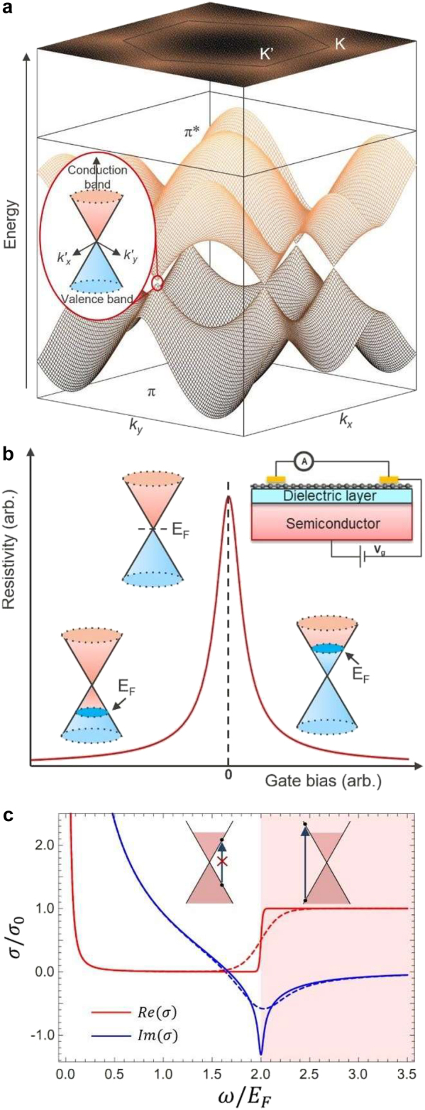
Photo-modulation is a promising strategy for contactless and ultrafast control of optical and electrical properties of photoactive materials. Graphene is an attractive candidate material for photo-modulation due to its extraordinary physical properties and its relevance to a wide range of devices, from photodetectors to energy converters. In this review, we survey different strategies for photo-modulation of electrical and optical properties of graphene, including photogating, generation of hot carriers, and thermo-optical effects. We briefly discuss the role of nanophotonic strategies to maximize these effects and highlight promising fields for application of these techniques.

Keywords: all-optical modulation; electrical properties; graphene; nanophotonic engineering; optical properties; photogating.


Figures

Figure 1:
Figure 1:
Electrical and optical properties of graphene. (a) Band structure of graphene. The top and bottom energy surfaces represent the conduction band (π* band) and the valence band (π band), respectively. Inset is the enlargement of the band structure near the Dirac point Κ0, showing the linear dispersion. (b) Resistivity of single-layer graphene as a function of an external gate bias showing the ambipolar electric field effect. Adapted with permission from [6]. (c) Optical conductivity of graphene, in units σ0=e2/4, as a function of frequency ω. The real part (Re(σ), red) and the imaginary part (Im(σ), blue) are plotted for low (T/EF=0.005, solid), and high (T/EF=0.05, dashed) temperature. The red shaded area denotes the regime of interband excitations. The inset schematic diagram explains the mechanism of Pauli blocking of photon absorption in graphene.
Figure 2:
Figure 2:
Hot carrier dynamics in graphene. (a) (i) Interband carrier transition upon optical excitation and the corresponding Fermi–Dirac distribution of carriers. (ii) Carrier–carrier scattering at a femtosecond timescale. (iii) A quasi-equilibrium state of carriers (electron and holes exhibit different temperatures). (iv) Interband thermalized carriers transition at a picosecond timescale, forming a single Fermi–Dirac distribution. (v) Thermal equilibrium of hot carriers with the lattice. (b) The variation of the electronic temperature with delay time. (c) The maximum electronic temperature as a function of fluence. Panel (a) adapted from [37], Panel (b) and (c) adapted from [38].
Figure 3:
Figure 3:
Overview of photo-modulation approaches. (a) Ultrafast optical modulation of graphene-only devices. The pump pulse generates a transient electronic response of graphene that in turns modulates the reflectance of the probe pulse. Controlling the time delay between the two pulses changes the modulation of the probe pulse. (b) Ultrafast electrical modulation of graphene p–n junction. Because the p-type and n-type graphene have different Seebeck coefficients, the absorbed light can increase the electronic temperature of graphene and further generate photocurrent due to photo-thermo-electric effects. The center of the illuminated region has the highest photocurrent. (c and d) Photo-modulation of graphene-based heterostructures. Two distinct ways can alter the graphene Fermi level and then change the photocurrent/resistivity via illumination: (c) by exchange of photo-generated charge carriers to/from an adjacent material, and (d) by the electrostatic screening of charges accumulated in a photoactive layer insulated from graphene via a dielectric layer, also called photo-gating.
Figure 4:
Figure 4:
Photo-modulation processes of graphene: PTO and PTE. (a and b) PTO effect in graphene and graphene/metal hybrid systems. Variation in the reflection spectra of graphene/Ag system in the (a) NIR and (b) far/mid-IR plasmonic regions for different electronic temperatures, Te, in graphene, where P, w, h are geometrical parameters and s is the spacings. All dielectrics in the structure (yellow regions in the insets) are taken to have a permittivity ε = 2. (c–f) PTE effect in graphene-based devices. Panel (a) and (b) adapted from [54]. (c) Dual-gated device incorporating boron nitride top-gate dielectric and spatially resolved photocurrent map at T = 40 K with laser wavelength 850 nm. Adapted with permission from [60]. (d) Device with three rectangular graphene regions with increasing widths; the white arrows in the photocurrent map (right panel) indicate that the photocurrent is generated from the graphene edge, the red arrows denotes the photocurrent along the straight edges’ regions of single layer graphene. Adapted with permission from [61]. (e) Device layout and photocurrent map in the transparent substrate device, with a flake that contains adjacent regions of single- and bi-layer graphene, as well as graphene–metal contact. Adapted with permission from [62]. (f) Waveguide integrated PTE graphene photodetector with a split-gate geometry where PTE current is generated by absorbing the waveguiding modes. Adapted with permission from [63].
Figure 5:
Figure 5:
Photo-modulation processes of graphene-based heterojunctions. (a) Schematic representation of band diagrams for the two kinds of photo-thermionic charge transfer processes in a graphene/TMD heterostructure: (left) 1μ-PTI, (right) 2μ-PTI. The red shaded area is the distribution of ultrafast thermalized HCs, ΦB is the Schottky barrier between graphene and TMDs [70]. (b) Graphene/MoTe2 photodevice where bands of MoTe2 bends upon the contact with graphene, creating a large-area 2D interface with facilitated electron injection to graphene. Adapted with permission from [, p. 2]. (c) Energy band alignment of graphene on Si/SiO2 substrate. The band bending at the Si/SiO2 interface induces electron–hole pairs separation. Under the gate bias, electrons (green) diffuse into the Si bulk, while holes (red) are trapped at the Si/SiO2 interface. The accumulation of photo-generated holes at the interface acts as an additional gate bias, increasing the Fermi level in graphene and its n-type doping. Adapted with permission from [94]. (d) (Left) Schematic of the graphene/silicon-on-insulator heterojunction device in photoconductive mode. (Right) Energy band diagrams of the photodetector under positive (top) and negative (bottom) vertical voltage showing opposite sign of the photogating in graphene. Adapted with permission from [91].
Figure 6:
Figure 6:
Schematic representation of the application domains for all-optical modulation of graphene.
Figure 7:
Figure 7:
Photodetection applications of graphene. (a) Waveguide integrated graphene photodetector with a narrow plasmonic waveguide for facilitated light absorption in graphene. Adapted with permission from [67]. (b) 3D GFET device before (left) and after (right) roll-up process. 3D photonic nanocavity significantly enhances light–matter interaction. Adapted with permission from [110]. (c) Schematic of the graphene/h-BN/Au heterostructure photodetector (left) where photoexcited hole-type carriers transport through the h-BN layer either by tunneling or thermal distribution (thermionic) transport (right). Adapted with permission from [75].
Figure 8:
Figure 8:
Energy conversion applications of graphene. (a) Graphene-TMDs vertical hybrid structure with graphene as transparent conductive electrode and WS2 as photosensitizer. (b) Graphene-based photovoltaic device with layered graphene and quantum dot (QD) films fabricated on transparent conducting indium tin oxide. (c) Top: Dynamic charge transfer when water is flowing over graphene arising from continuous doping and un-doping of the photoexcited carriers. Bottom: Schematic band profile of graphene–silicon nanogenerator. (d) A graphene-based nanogenerator harvesting light energy and enhanced voltage output under flow of water drops. Panel (a) adapted with permission from [119], Panel (b) adapted with permission from [123], Panel (c) and (d) adapted with permission from [12].
Figure 9:
Figure 9:
Data processing applications of graphene. (a) Schematic of biological synaptic transmission. (b) Artificial axon-multi-synaptic network based on graphene-SWCNTs hybrids under multiple light spikes. Inset image is the band diagram of graphene/SWCNTs interface before and after illumination. (c) The dynamic photoresponse of the NOR logic operation of the network. (d) Schematic illustrations of biological tactile/visual sensory systems. (e) Schematic structure of a graphene/MoS2 heterostructure-based artificial synapse. The inset is the band diagram of the graphene/MoS2 mechano-optoelectronic transistor at separation state. Panel (b) and (c) are adapted with permission from [152], Panel (a), (d) and (e) are adapted with permission from [13].
Figure 10:
Figure 10:
Light-modulation applications of graphene. (a) Graphene mode-locked ultrafast laser: a graphene SA is inserted between two fiber connectors. An erbium-doped fiber (EDF) is the gain medium, pumped by a laser diode (LD) with a wavelength-division multiplexer (WDM). An isolator (ISO) maintains unidirectional operation, and a polarization controller (PC) optimizes mode-locking. (b) Measured transmissivity transients for multilayer graphene. The open circles are the experimental data and the solid curve is analytical fit to the data using exponentials with time constants t1 and t2. The fast relaxation time t1 corresponds to carrier–carrier intraband scattering rates and the slow relaxation time t2 correlates with electron–hole interband recombination. (c) Nonlinear absorption of graphene films vs excitation intensity for different numbers of graphene layers. The dots are the experimental data and the solid curves are analytical fits to the data using Eq. (4). (d) Modulation depth and saturated carrier density versus number of graphene layers. (e) Graphene resonators array placed on the temperature-controlled stage with electrostatic gating for emissivity measurements. (f) Carrier density dependence of change in emissivity with respect to the charge neutral point (CNP) for 40 nm graphene nanoresonators (inset) at 250 °C. Panel (a) is adapted with permission from [7]; Panel (b)–(d) are adapted with permission from [156]. Panel (e) and (f) are adapted with permission from [160].

References

    1. Das Sarma S., Adam S., Hwang E. H., Rossi E. Electronic transport in two-dimensional graphene. Rev. Mod. Phys. . 2011;83(2):407–470. doi: 10.1103/RevModPhys.83.407. - DOI
    1. Falkovsky L. A. Optical properties of graphene. J. Phys.: Conf. Ser. . 2008;129:012004. doi: 10.1088/1742-6596/129/1/012004. - DOI
    1. Papageorgiou D. G., Kinloch I. A., Young R. J. Mechanical properties of graphene and graphene-based nanocomposites. Prog. Mater. Sci. . 2017;90:75–127. doi: 10.1016/j.pmatsci.2017.07.004. - DOI
    1. Balandin A. A., Ghosh S., Bao W., et al. Superior thermal conductivity of single-layer graphene. Nano Lett. . 2008;8(3):902–907. doi: 10.1021/nl0731872. - DOI - PubMed
    1. Elias D. C., Nair R. R., Mohiuddin T. M. G., et al. Control of graphene’s properties by reversible hydrogenation: evidence for graphane. Science . 2009;323(5914):610–613. doi: 10.1126/science.1167130. - DOI - PubMed

LinkOut - more resources