. 2024 Jan 9;13(12):2117-2125.
doi: 10.1515/nanoph-2023-0651. eCollection 2024 May.

Spatio-spectral control of coherent nanophotonics

Affiliations

Spatio-spectral control of coherent nanophotonics

June Sang Lee et al. Nanophotonics. .

Abstract

Fast modulation of optical signals that carry multidimensional information in the form of wavelength, phase or polarization has fueled an explosion of interest in integrated photonics. This interest however masks a significant challenge which is that independent modulation of multi-wavelength carrier signals in a single waveguide is not trivial. Such challenge is attributed to the longitudinal direction of guided-mode propagation, limiting the spatial separation and modulation of electric-field. Here, we overcome this using a single photonic element that utilizes active coherent (near) perfect absorption. We make use of standing wave patterns to exploit the spatial-degrees-of-freedom of in-plane modes and individually address elements according to their mode number. By combining the concept of coherent absorption in spatio-spectral domain with active phase-change nanoantennas, we engineer and test an integrated, reconfigurable and multi-spectral modulator operating within a single element. Our approach demonstrates for the first time, a non-volatile, wavelength-addressable element, providing a pathway for exploring the tunable capabilities in both spatial and spectral domains of coherent nanophotonics.

Keywords: active photonics; phase-change materials; photonic spatio-spectral reconfiguration.


Conflict of interest statement

Conflict of interest: Authors state no conflicts of interest.

Figures

Figure 1:
Figure 1:
PSR in a single waveguide. (A) While conventional PICs (left) can carry the multiple optical signals at a single waveguide, the modulation (w 1 and w 2) of such signals is non-selective. However, standing-wave PICs (right) can bring the additional capability of selectively modulating wavelength-multiplexed signals without requiring extra waveguides or electro-modulators. This is enabled by photonic spatio-spectral reconfiguration (PSR) of active elements within the standing-wave cavities. (B) Schematic and electric-field distribution of an enlarged view for a single Si waveguide when wavelength-selective standing waves are formed due to interference of counter-propagating light (λ 1 (1538 nm) – λ 2 (1578 nm)). The active nanoantenna of 25 nm thickness, 100 nm width, and 250 nm length is placed on the waveguide. Spatial positions (x 1x 2) of standing waves are shifted at different spectral positions (λ 1λ 2), and such spatio-spectral modulation allows the light to pass through the nanoantenna undisturbed at one wavelength (λ 1) but interacts with it at the other wavelength (λ 2). Note that the field profile is an enlarged view from the full-field distribution in Supplementary Figure 1. Scale bar is 500 nm. (C) Wavelength-selectively reconfigurable optical transmission (i.e. absorption) is achieved at λ 2 upon switching the nanoantenna between on (amorphous) and off (crystalline) states, while the absorption at λ 1 is suppressed. Inset shows a cross-section of normalized absorption profile for a Si waveguide with the active nanoantenna, which exhibits wavelength-selective absorption. Scale bar is 200 nm.
Figure 2:
Figure 2:
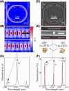
PSR in a microring resonator. (A and B) Electric-field distribution of a racetrack microring resonator when the counter-propagating waves from two input arms generate standing waves. Standing waves are out-of-phase depending on the incoming wavelength so that the active nanoantenna (i.e. GST) is invisible to the odd-mode (top, 1505 nm (λ 1)), but evanescently coupled to the even-mode (bottom, 1528 nm (λ 2)). Scale bars are 2 µm and 500 nm, respectively. (C) Absorption spectrum of the active nanoantenna that shows a selectively high absorption at the even-mode. (D and E) SEM scan of a racetrack microring resonator with active nanoantenna deposited on a waveguide. Scale bars are 10 µm and 500 nm, respectively. (F) Transmission spectra of a racetrack mirroring resonator when the nanoantenna is in (blue, ON) as-deposited amorphous and (red, OFF) crystalline phase after heating the device onto a hot-plate.
Figure 3:
Figure 3:
Wavelength-selectively reconfigurable system by optical pulses. (A) Enlarged transmission spectra of the PSR system with active nanoantennas (GST/Au) at the odd-mode (left, λ 1) and the even mode (right, λ 2), respectively. The set (220 pJ for 10 ns + 1.8 nJ for 300 ns with repetition of 50 times) and reset (220 pJ for 10 ns) optical pulses are sent to the device at the even-mode wavelength so that the reconfigurable transmission levels are only achieved in the even-mode wavelength. (B) Switching cyclability of wavelength-selective switching as in A. (C) Enlarged transmission spectra of multi-level wavelength-selective operations at the odd-mode (left, λ 1) and the even-mode (right, λ 2), respectively. The wavelength of optical pulses is at the even-mode and the number of such set pulses vary from 10 to 50. (D) Switching cyclability of wavelength-selective multi-level operations as in C.
Figure 4:
Figure 4:
Reconfigurable multi-spectral filter in a single element. (A) Colorized SEM image of an enlarged view of the active nanoantennas (GST/Au) on a waveguide for PSR system. The separation between two nanoantennas is 460 nm. Wavelength-selective input signals (P λ1 and P λ2) are independently modulated by weighting coefficients of each nanoantenna (G left and G right). (B) Absorption profile of the PSR system with double nanoantennas, where the odd-mode (top, 1528 nm (λ 1)) couples with the left nanoantenna and the even-mode (bottom, 1550 nm (λ 2)) couples with the right nanoantenna. (C) Absorption spectra at each nanoantenna showing the wavelength-selective absorption contrast. (D and E) Enlarged transmission spectra of intensity-tunable multi-spectral filter at the odd-mode (left, 1536 nm (λ 1)) and the even-mode (right, 1542 nm (λ 2)), respectively. Reset pulses of 220 pJ (10 ns) with varying the pulse duration from 10 to 25 ns are used to provide wavelength-selective multi-levels under (D) odd-mode and (E) even-mode illumination. The piecewise set pulse of (220 pJ for 10 ns + 1.8 nJ for 300 ns with repetition of 50 times) is used for initializing the transmission level.

References

    1. Bogaerts W., et al. Programmable photonic circuits. Nature . 2020;586:207–216. doi: 10.1038/s41586-020-2764-0. - DOI - PubMed
    1. Feldmann J., et al. Parallel convolutional processing using an integrated photonic tensor core. Nature . 2021;589:52–58. doi: 10.1038/s41586-020-03070-1. - DOI - PubMed
    1. Cheng Z., Ríos C., Pernice Wolfram H. P., Wright C. D., Bhaskaran H. On-chip photonic synapse. Sci. Adv. . 2017;3(9):20230651. doi: 10.1126/sciadv.1700160. e1700160. - DOI - PMC - PubMed
    1. Peng H. T., Nahmias M. A., Lima T. F. d., Tait A. N., Shastri B. J. Neuromorphic photonic integrated circuits. IEEE J. Sel. Top. Quantum Electron. . 2018;24(6):1–15. doi: 10.1109/jstqe.2018.2840448. - DOI - PMC - PubMed
    1. Tait A. N., et al. Neuromorphic photonic networks using silicon photonic weight banks. Sci. Rep. . 2017;7:7430. doi: 10.1038/s41598-017-07754-z. - DOI - PMC - PubMed

LinkOut - more resources