. 2023 Jan 10;12(8):1469-1479.
doi: 10.1515/nanoph-2022-0584. eCollection 2023 Apr.

Fabrication of quantum dot and ring arrays by direct laser interference patterning for nanophotonics

Affiliations

Fabrication of quantum dot and ring arrays by direct laser interference patterning for nanophotonics

Yun-Ran Wang et al. Nanophotonics. .

Abstract

Epitaxially grown semiconductor quantum dots (QDs) and quantum rings (QRs) have been demonstrated to be excellent sources of single photons and entangled photon pairs enabling applications within quantum photonics. The emerging field of QD-based nanophotonics requires the deterministic integration of single or multiple QD structures into photonic architectures. However, the natural inhomogeneity and spatial randomness of self-assembled QDs limit their potential, and the reliable formation of homogeneous and ordered QDs during epitaxy still presents a challenge. Here, we demonstrate the fabrication of regular arrays of single III-V QDs and QRs using molecular beam epitaxy assisted by in situ direct laser interference patterning. Both droplet epitaxy (DE) GaAs/AlGaAs QDs and QRs and Stranski-Krastanov (SK) InAs/GaAs QDs are presented. The resulting QD structures exhibit high uniformity and good optical quality, in which a record-narrow photoluminescence linewidth of ∼17 meV from patterned GaAs QD arrays is achieved. Such QD and QR arrays fabricated through this novel optical technique constitute a next-generation platform for functional nanophotonic devices and act as useful building blocks for the future quantum revolution.

Keywords: direct laser interference patterning; droplet epitaxy; molecular beam epitaxy; quantum dots; quantum rings.


Figures

Figure 1:
Figure 1:
Schematic configuration of the four-beam DLIP-MBE setup. The insect shows a CMOS camera image of the four superimposed beams on an InGaN wafer.
Figure 2:
Figure 2:
AFM micrographs of (a) and (b) square arrays of nanoislands with different sizes on AlGaAs surface induced by in situ four-beam DLIP. 2.5 ML Ga were deposited on the nanoisland-templated surface at T s = 100 °C with (c) multiple Ga droplets nucleate at large nanoislands, and (d) single or pair Ga droplets nucleate at small nanoislands. The insets display the enlarged 3-D AFM images.
Figure 3:
Figure 3:
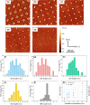
AFM images of crystallised 2 ML GaAs QDs grown at nanoisland-templated surfaces with different diameters of nanoislands (a)–(e) 250, 150, 100, 80 and 50 nm accordingly. (f)–(j) Corresponding histograms of QD height distribution. (k) QD occupancy per nanoisland and QD height in response to the diameter of the nanoisland.
Figure 4:
Figure 4:
AFM micrographs of 2 ML GaAs QD nanostructure arrays grown at different T s and As BEPs for crystallisation of (a) T s = 200 °C, BEP = 2.4 × 10⁻⁴ mbar, (b) T s = 400 °C, BEP = 1 × 10⁻⁴ mbar, (c) T s = 400 °C, BEP = 2.3 × 10⁻⁵ mbar, and (d) T s = 400 °C, BEP = 1.4 × 10⁻⁶ mbar. (e)–(h) The corresponding enlarged AFM images of single QD structures as marked in (a)–(d), respectively. (i)–(l) Line scans of each QD structure.
Figure 5:
Figure 5:
Graph of various structures formed at different crystallisation temperatures and As BEPs. ◆: single rings, ▲: ring-disks, ★: coupled QDs, ■: single QDs. Red symbols represent our experimental data, and black symbols refer to experimental data from other reported work [33, 35, 41, 42, 43].
Figure 6:
Figure 6:
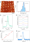
Characterisation of patterned GaAs QD structures. (a) 3-D AFM micrograph of a regular array of single GaAs/AlGaAs QDs. (b) Corresponding QD height histogram. (c) The ensemble-PL spectrum of the patterned GaAs QD arrays with low excitation power at 60 ± 5 K. (d) Normalised excitation power-dependent PL spectra. (e) Integrated PL intensity depending upon the excitation power density. The solid line defines the slope k = 1.09. (f) PL spectrum of the patterned GaAs QR arrays with an excitation power of 10 µW.
Figure 7:
Figure 7:
AFM micrographs of (a) InAs QDs formed on the nanoisland-templated surface with a total InAs coverage of 1.7 ML, and (b) the magnified AFM image of a single nanoisland site. (c) Line scans across the direction as marked in (b).
Figure 8:
Figure 8:
Characterisation of patterned InAs QDs. (a) 3-D AFM micrograph of an array of single InAs/GaAs QDs induced by in situ DLIP. (b) Histogram of QD height distributions. (c) Low-temperature PL spectrum with an excitation power of 1.5 µW.

References

    1. Davanco M., Liu J., Sapienza L., et al. Heterogeneous integration for on-chip quantum photonic circuits with single quantum dot devices. Nat. Commun. . 2017;8(889):20220584. doi: 10.1038/s41467-017-00987-6. - DOI - PMC - PubMed
    1. Senellart P., Solomon G., White A. High-performance semiconductor quantum-dot single-photon sources. Nat. Nanotechnol. . 2017;12(11):1026–1039. doi: 10.1038/nnano.2017.218. - DOI - PubMed
    1. Lu C. Y., Pan J. W. Quantum-dot single-photon sources for the quantum internet. Nat. Nanotechnol. . 2021;16(12):1294–1296. doi: 10.1038/s41565-021-01033-9. - DOI - PubMed
    1. Hennessy K., Badolato A., Winger M., et al. Quantum nature of a strongly coupled single quantum dot-cavity system. Nature . 2007;445(7130):896–899. doi: 10.1038/nature05586. - DOI - PubMed
    1. Ellis B., Mayer M., Shambat G., et al. Ultralow-threshold electrically pumped quantum-dot photonic-crystal nanocavity laser. Nat. Photonics . 2011;5(5):297–300. doi: 10.1038/nphoton.2011.51. - DOI

LinkOut - more resources