. 2024 Jun 26;13(19):3749-3763.
doi: 10.1515/nanoph-2024-0258. eCollection 2024 Aug.

Multilayer all-dielectric metasurfaces expanding color gamut

Affiliations

Multilayer all-dielectric metasurfaces expanding color gamut

Xin Gu et al. Nanophotonics. .

Abstract

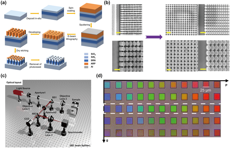
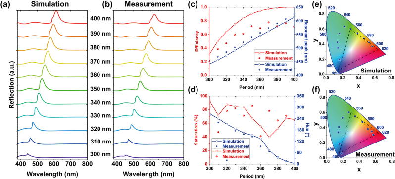
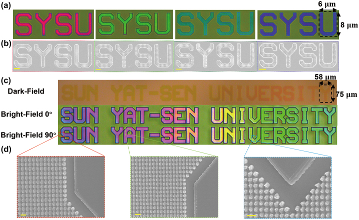
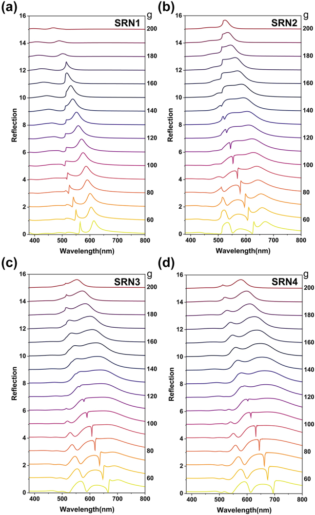
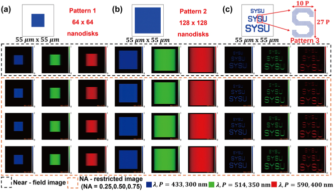
Structural color, arising from the interaction between nanostructures and light, has experienced rapid development in recent years. However, high-order Mie resonances in dielectric materials often induce unnecessary sub-peaks, particularly at shorter wavelengths, reducing the vibrancy of colors. To address this, we have developed a multilayer dielectric metasurface based on silicon-rich silicon nitride (SRN), achieving expanded color gamut through precise refractive index matching and suppression of high-order resonances. This strategy introduces more design dimensions and can reduce the complexity of material deposition. It enables the generation of vibrant colors in a 3 × 3 array, with a resolution of approximately 25,400 dpi, demonstrating its potential applications in displays.

Keywords: high-order resonances; metasurfaces; multipole expansion; silicon-rich silicon nitride; structural color.


Conflict of interest statement

Conflict of interest: Authors state no conflicts of interest.

Figures

Figure 1:
Figure 1:
Multilayer all-dielectric metasurface design and optical properties. (a) Structural design of the multilayer all-dielectric metasurface under normally visible illumination. Each unit cell consists of a 100-nm thick (H 1) SiO2 capping layer, a 150-nm thick (H SRN) SRN spacer layer, and a 50-nm thick (H 3) SiN x layer from top to bottom. (b) Dispersion characteristics of SiN x and SRN in the visible spectral band (the ratios of SiH4 and N2 gases are measured in sccm).
Figure 2:
Figure 2:
Color representations and optical characteristics for (a) all-SiN x structures, (b) all-SRN structures and (c) multilayer all-dielectric structures (each shown 55 nanodisks with P from 300 to 400 nm in 10-nm step and g from 300 to 400 nm in 20-nm step). (d–f) Simulated reflection spectra of nanodisks with a period of 350 nm and a diameter of 200 nm. The insets show the electric field and magnetic field distribution of all-SiN x structures at 437 nm (red box)/533 nm (green box), all-SRN structures at 458 nm (yellow box)/554 nm (purple box) and multilayer all-dielectric structures at 458 nm (blue box)/514 nm (brown box), respectively. (g–i) Multipolar decomposition of scattering cross-sections in terms of electric dipole (ED), magnetic dipole (MD), electric quadrupole (EQ), and magnetic quadrupole (MQ).
Figure 3:
Figure 3:
Influences on tunable refractive index SRN materials for the design of multilayer all-dielectric metasurface. (a) The 1931 CIE diagram for the structures of different refractive indices of middle layer (SRN1, SRN2, SRN3 and SRN4) with different SRN and SiN x thickness ratios(in 25-nm step). (b) The 1931 CIE diagram for the structures of different refractive indices of middle and bottom layers (SRN1, SRN2, SRN3 and SRN4) with different SRN a and SRN b thickness ratios(in 25-nm step). (c, d) Calculated multipolar decomposition of scattering cross section distribution of ED, MD and EQ, MQ modes according to (a) and (b) (pointed by the arrow). (e) The 1931 CIE diagram for the structures optimized of different refractive indices of middle (SRN1, SRN2, SRN3 and SRN4) and bottom (SiN x and SRN1) layers according to (a) and (b) (pointed by the arrow).
Figure 4:
Figure 4:
Fabrication and measurement of the multilayer SRN metasurface. (a) Schematic of the sample fabrication process. (b) The SEM images of the photoresist before etching and the multilayer SRN metasurface, scale bars are both 500 nm. (c) Schematic illustrating the optical setup for measuring spectra with spectrometer and capturing color images with CCD camera. (d) Measured color palette with varying periods and gaps. The size of each color palette is 25 μm × 25 μm.
Figure 5:
Figure 5:
Simulated and measured results of pixels indicated by dashed boxes in Figure 3(d) with periods varying from 300 to 400 nm when the gap is fixed at 150 nm. (c, d) The comparison between simulated and measured results is shown for (c) the efficiency and resonant peak of the reflection spectra and (d) the hue and saturation of the reflected colors. The solid line corresponds to the simulated data, while the scattered dots represent the measured results. (e, f) The corresponding CIE 1931 chromaticity coordinates based on (c) simulated spectra and (d) measured spectra respectively.
Figure 6:
Figure 6:
Colorful images printed by the SRN-based multilayer nanostructures. (a) The reflected images for fabricated “SYSU” patterns with four sizes. (b) Top-view SEM images for the patterns “SYSU” with period of 400 nm (highlighted by red box), 350 nm (highlighted by green box), 300 nm (highlighted by blue box) and 250 nm (highlighted by purple box) respectively. The scale bar is 2 μm. (c) The color-graded images for fabricated “SUN YAT-SEN UNIVERSITY” patterns of dark field, bright field with 0° and bright field with 90°, respectively. (d) Side-view (45°) SEM images for the patterns “S” with period of 400 nm and diameter of 290 nm (highlighted by red box), “A” with period of 380 nm and diameter of 210 nm (highlighted by green box) and “V” with period of 335 nm and diameter of 176 nm (highlighted by blue box), respectively. The scale bar is 1 μm.
Figure 7:
Figure 7:
Multipolar decomposition of scattering cross-sections in terms of electric dipole (ED), magnetic dipole (MD), electric quadrupole (EQ), and magnetic quadrupole (MQ) in Table 6.
Figure 8:
Figure 8:
Simulated reflection spectra of nanodisks with a period of 350 nm and a diameter of 200 nm (the total thickness of three layers is set as 300 nm, SRN1 = 150 nm and SiN x = 40/50/60/70 nm).
Figure 9:
Figure 9:
Optical properties of SRN-based metasurfaces and detailed analysis of multipolar scattering. (a) Simulated reflection spectra (b) absorption (calculated by A = 1 − TR) and (c) The corresponding CIE 1931 chromaticity coordinates based on the with the middle layer (d) SRN1, (e) SRN2, (f) SRN3 and (g) SRN4 of nanodisks with a period of 350 nm and a diameter of 200 nm. Calculated multipolar decomposition of scattering cross section when the middle layer is (d) SRN1, (e) SRN2, (f) SRN3 and (g) SRN4 and (h) & (i) Magnifying distribution of MD and EQ mode for various material of middle layer.
Figure 10:
Figure 10:
Optical properties of nanodisks with varied refractive indices. (a) Simulated reflection spectra with the refractive indices of bottom layer (b) 1.8, (c) 2.0, (d) 2.2 and (e) 2.4 of nanodisks with a period of 350 nm and a diameter of 200 nm. Calculated multipolar decomposition of scattering cross section when the refractive index of bottom layer is ((b) 1.8, (c) 2.0, (d) 2.2 and (e) 2.4). (g), (f) Magnifying distribution of MD and EQ mode for various refractive indices of bottom layer.
Figure 11:
Figure 11:
Simulated reflection spectra with (a) SRN1, (b) SRN2, (c) SRN3 and (d) SRN4 of nanodisks with a period of 350 nm and gap g from 50 nm to 200 nm (in 10-nm steps).
Figure 12:
Figure 12:
Imaging analysis of multilayer all-dielectric nano-patterns for near-filed and NA-restricted conditions. (a) The images of 64 × 64 pixels-based square patterns with different wavelengths and NA. (b) The images of 128 × 128 pixels-based square patterns with different wavelengths and NA. (c) The images of “SYSU” patterns with different wavelengths and NA. The pattern scale is related to resolution (the number of nanodisks) and the period of nanodisks (the top, middle and bottom layers were set as 100 nm SiO2, 150 nm SRN1 and 50 nm SiN x , the gap g of 150 nm, respectively).

References

    1. Rouw R., Scholte H. S. Increased structural connectivity in grapheme-color synesthesia. Nat. Neurosci. . 2007;10(6):792–797. doi: 10.1038/nn1906. - DOI - PubMed
    1. Li Z., et al. Meta-optics achieves RGB-achromatic focusing for virtual reality. Sci. Adv. . 2021;7(5):eabe4458. doi: 10.1126/sciadv.abe4458. - DOI - PMC - PubMed
    1. Dean N. Colouring at the nanoscale. Nat. Nanotechnol. . 2015;10(1):15–16. doi: 10.1038/nnano.2014.316. - DOI - PubMed
    1. Peters A. T., Freeman H. S., editors. Modern Colorants: Synthesis and Structure . Dordrecht: Springer Netherlands; 1995.
    1. Daqiqeh Rezaei S., et al. Nanophotonic structural colors. ACS Photonics . 2021;8(1):18–33. doi: 10.1021/acsphotonics.0c00947. - DOI

LinkOut - more resources