Review
. 2022 Feb 24;11(6):1083-1108.
doi: 10.1515/nanoph-2021-0823. eCollection 2022 Feb.

Computing metasurfaces for all-optical image processing: a brief review

Affiliations
Review

Computing metasurfaces for all-optical image processing: a brief review

Shanshan He et al. Nanophotonics. .

Abstract

Computing metasurfaces are two-dimensional artificial nanostructures capable of performing mathematical operations on the input electromagnetic field, including its amplitude, phase, polarization, and frequency distributions. Rapid progress in the development of computing metasurfaces provide exceptional abilities for all-optical image processing, including the edge-enhanced imaging, which opens a broad range of novel and superior applications for real-time pattern recognition. In this paper, we review recent progress in the emerging field of computing metasurfaces for all-optical image processing, focusing on innovative and promising applications in optical analog operations, image processing, microscopy imaging, and quantum imaging.

Keywords: all-optical image processing; computing metasurface; edge detection; microscopy imaging; optical differential operation; quantum imaging.


Figures

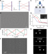
Figure 1:
Figure 1:
Three dielectric gradient metasurface optical elements (DGMOE) for the manipulation of light [49]. (A) Schematic of a conventional glass axicon generating a Bessel beam (left) and a DGMOE axicon featuring an ultrathin patterned layer of silicon on a quartz substrate (right). (B) Scanning electron microscopy (SEM) image of the fabricated DGMOE axicon constructed from Si nanoantennas. (C) Schematic view of a periodic 120-nm-wide and 100-nm-high Si nanobeam array on fabricated ultrathin wave plates. (D) Simulated phase retardation of a TM-polarized wave with respect to a TE-polarized wave for nanobeam arrays with widths of 100 nm (blue), 120 nm (red), 140 nm (green), with the same thickness of 100 nm and duty cycle of 60% . Measurements of the phase retardation (red squares) obtained with an array of 120-nm widths (SEM image in inset) show good agreement with the simulations. The phase retardation of the wave plate varies from 0.4π to 1.2π with the wavelength from 490 to 700 nm. In contrast, the phase retardation is approximately equal to 0.05π for a 100-nm-thick calcite film (dashed black line). (E) Discretized (solid line) and continuous (dashed line) phase profile of a DGMOE grating for illumination with LCP light (red) and RCP light (green). (F) SEM image of the fabricated grating. (G) Measured diffraction patterns from the grating under illumination with right circular polarization (top), linear polarization (middle), and left circular polarization (bottom) at λ=550 nm.
Figure 2:
Figure 2:
Wave-based computational metamaterials [18]. (A) The computational metamaterial system consists of three cascaded sub-blocks: (i) the Fourier transform sub-block GRIN(+), (ii) a suitably customized metasurface (MS) spatial filter in the Fourier domain, and (iii) Fourier inverse transform sub-block GRIN(−). The length Lg of GRIN(+) and GRIN(−) is 12λ0 . (+) and (−), respectively, indicate that the permittivity and permeability are positive and negative. GRIN(−) has the inverse function of GRIN(+). The thin metastructure screen with thickness Δ=λ0/3 and width W10λ0 is sandwiched between two GRIN structures with positive and negative parameters. Two designs are proposed for the middle metastructure: a thin MS formed of a single layer with prescribed dielectric constant and permeability [left inset, real part (red) and imaginary part (blue) with material parameters] and a realistic metatransmit-array (MTA) is formed by three sub-layers made of two alternating materials (Si and AZO). Their volume filling fractions have a properly regulated non-uniform distribution, and they have the required loss to provide the desired attenuation (right inset). (B) The metamaterial block performs a conceptual illumination of the required mathematical operations in the spatial Fourier domain. Input arbitrary wave signals propagate through the thin planar metamaterial block, in which the first-order differential operation can be performed, and a waveform satisfying the operation can be generated at output.
Figure 3:
Figure 3:
Illustration of the polarization evolutions on Poincaré sphere and the PB phases included [73]. (A) The induced PB phase varies periodically with the rotation of optical axes, and this variation is in the opposite directions when left- or right-circularly polarized light passes through the metasurface. The red and blue arrows indicate left- and right-circularly polarized lights. The incident light gets a 2 θ phase, which is double the orientation angle of the optical axis (slow) and half of the solid angle enclosed by the polarization evolving routes. (B) By controlling the local orientation of the optical axis, any desired phase can be obtained.
Figure 4:
Figure 4:
Schematic and experimental demonstration of photonic SHE in a structured metasurface [76]. (A) represent the transition of the spin state when circularly polarized light is transmitted through a structured metasurface with a spin-dependent PB phase gradient ΦG . The short line marked on the metasurface indicates the local optical axis direction. The green arrows show the wave vectors. For the incident left-handed circularly polarized light ( σ+ , red) and right-handed circularly polarized light ( σ , blue), the metasurface produces the opposite ΦG and the opposite spin-dependent momentum displacement. (B) Microscopic photograph of the metasurface. (C) A schematic illustration of the detailed geometry and local optical axis (slow axis) of the metamaterial in a period (20 mm). (D) The mapping relationship between momentum displacement Δk and induced real space displacement Δx . After the linearly polarized beam passes through two metasurfaces with completely opposite rotation rates Ω , charge-coupled device records the intensity and the corresponding S3 parameters, the observation plane is 10 cm away from the metasurface. The experimental results of the metamaterial with Ω=π/20 rad μm1 are shown in (E) and (F). (G) and (H) The experimental results of the metamaterial with Ω=π/20 rad μm1 .
Figure 5:
Figure 5:
Vortex-phase metasurface for edge detection [132]. (A) The incident circularly polarized light passes through the metasurface, and the polarization chirality is reversed. For the incident RCP, the metasurface will produce a constant phase distribution and intensity distribution on the output beam, realizing a two-dimensional spatial differentiation operation. (B) Schematic of the all-dielectric metasurface spatial filter designed to realize photonic spin-multiplexing function. Inset: Perspective and top view of a metasurface unit cell formed by amorphous TiO2 nanopillars on a silica substrate. (C) Top view and oblique view of SEM image of TiO2 nanopillar array. Scale bar: 1 μm. (D)–(G) The bright field images of the resolution test chart under the incident LCP light and the edge-enhanced phase contrast images with the incident RCP light at wavelengths of 480, 530, 580, and 630 nm. The inset shows the handedness of the incident light. Scale bar: 100 μm.
Figure 6:
Figure 6:
Nonlocal metasurfaces for first-derivative and second-derivative operations [19]. (A) Schematic of a metasurface consisting of a periodic array of resonant particles in the xy plane, formed by split ring resonators (SRR) parallel to the xz plane (magnetic dipole moment parallel to the y axis). The metasurface is excited by TM polarized waves propagating in the xz plane. The metasurface with broken x and z symmetry results in asymmetric responses with respect to ±kx , achieving the required first-derivative operation. (B) The designed metasurface structure with 90° rotational symmetry to implement the second derivative in 2D. (C) The relationship between the transmission and the incident angle of the metasurface (solid line) and the ideal first-derivative operation (dashed line) in (A). The selected distance of the transmission reference plane results in a 0° transmission phase at normal incidence. (D) The relationship between the transmittance of the metasurface and the incident angle (solid line) for the response to the ideal second-derivative operation (dashed line). The selected distance of the transmission reference plane results in a 180° transmission phase at normal incidence. (E) The input image used to test the response of the metasurface at f=0.98f0 , where f0 is the resonance frequency of the unmodulated metasurface. In the process of signal processing, the input signal needs to be discretized, and the pixel size in each direction is 0.86λ . (F) The output 1D edge image in the x direction by the metasurface when the x -polarized wave is illuminated. (G) The output 1D edge image in the y direction when the y -polarized wave is illuminated. (H) The 2D edge image obtained when unpolarized light from the normal direction is used to illuminate the metasurface.
Figure 7:
Figure 7:
Broadband edge detection based on high-efficiency PB phase metasurface [96]. (A) Experimental setup: two lenses form a 4f system, and the metasurface (sample) is placed between P1 and P2. L: lens, P: polarizer. (B) The metasurface period Λ of the imaging experiment is 8000 μm. The illumination wavelengths are respectively 430, 500 and 670 nm. The first row shows the images without the analyzer after the sample, and the second row shows the edge image with the crossed polarizers. (C) Photograph of a sample with a diameter of 2.54 cm (left), with a metasurface pattern area of 8 × 8 mm (scale bar: 5 mm). The optical image of the marked sample (right), the red lines indicate the direction of the nanostructure in a period. The inset is the SEM image of the nanostructure (scale bar: 500 nm). (D)–(G) Various resolutions of edge detection with different phase gradient periods: 500, 750, 1000, and 8000 μm, at the wavelength of 500 nm. The first row is photographs of different metasurface samples. The second row is polarized images of the samples (scale bar, 125 μm). The third row is two separated LCP and RCP images without the analyzer. The fourth row is edge images corresponding to different resolutions.
Figure 8:
Figure 8:
Edge-enhanced image based on quantum imaging violates Bell inequality [42]. (A) Perform imaging settings for Bell inequality test. A β -barium borate (BBO) crystal pumped by an ultraviolet laser serves as a source of entangled photons. The beam splitter (BS) separates pairs of entangled photons. The intensified charge coupled device (ICCD) camera acquires the ghost image of the phase object in spatial light modulator (SLM 1) placed on the first photon path. Four different spatial filters implement nonlocal filtering. These spatial filters and the camera are placed in another optical path. By being triggered by single-photon avalanche diode (SPAD), the camera acquires a coincident image that can be used to perform the Bell test. (B) The coincidence of the same phase circle obtained by using four phase filters in different directions counts a single image. (C) The correspondence between the phase filter used and the specific observation of the object acquired in a single image is highlighted, by a ring-like region of interest (ROI) along the edge of the phase circle object within (B).
Figure 9:
Figure 9:
Quantum switchable edge detection based on PB phase metasurface [43]. (A) Schematic of experimental setup for switchable quantum edge imaging. (B) The polarization switch controls the coincidence image: Polarization |H> is OFF state, corresponding to the bright field mode “solid cat” (the first row shows simulation and experimental imaging); |V> state is ON state, corresponding to edge detection mode “outlined cat” (the second row shows simulation and experimental imaging). (C) Experimental setup for metasurface enabled quantum edge detection. BDM, broadband dielectric mirror; PPKTP crystal, periodically polarized KTiOPO4 crystal; DPBS, dual-wavelength polarization beam splitter; PBS, polarization beam splitter; DM, dichroic mirror; FC, fiber coupler; BPF, band-pass filter; DHWP, dual-wavelength 1/2 wave plate; QWP, 1/4 wave plate; SPAD, single photon avalanche detector; ICCD, intensified charge coupled device. The blue (red) light path presents the 405 nm (810 nm) light. The edge detection switch is on the forecast end, and the edge detection system is installed on the imaging end. (D) Coincident edge image of photon pair in external trigger mode and the one-dimensional intensity distribution along the white dashed line. (E) Edge image in internal trigger mode and the one-dimensional intensity distribution along the white dashed line.
Figure 10:
Figure 10:
Nanophotonics enhanced coverslip (NEC) for high-contrast intensity images of phase objects [126]. (A) Measuring equipment for optical transfer function of fabricated NEC. The linear polarizer selects the desired polarization direction relative to direction of the grating fringes on the NEC (inset marked by dotted line). The output lens produces a Fourier plane image. The other inset reveals the nanostructure of NEC cross-section, in which design parameters are t1=100 nm, t2=40 m, d=200 nm, and p=400 nm. When the light of wavelength λ=650 nm is incident vertically, the simulated electric field distribution ( yˆ component) of the induced standing wave in the waveguide is displayed. (B) The normalized two-dimensional modulation transfer function measured when the incident light (wavelength of λ=637 nm) is polarized parallel to ( y -pol) and perpendicular to the silver grating fringe ( x -pol). (C) The cross-sectional view along the dotted line (red) in (B), which highlights the suppression of low k in the direct beam. The corresponding simulated profile of the s -polarization (blue) and the spatial frequency of the incident beam (grey) are given for comparison with experimental measurements. (D) Experimental device for phase object microscopy imaging: The wavelength of the light source is 637 nm, and the incident light field whose polarization direction is parallel to the grating line is generated through the collimator and polarizer. The culture dish of Human cancer cells (HeLa) is fixed on top of NEC. (E)–(F) Images obtained with the same cell area with and without NEC under two different tilts (no tilt in (E), tilt 3° in (F)) relative to the incident light. (G)–(H) A conventional microscope image of the same cell using DIC and fluorescence. The blue area in the fluorescence image highlights the cell nucleus. (I) The magnified image shown by the number in (F) to (H) for NEC tilted at 3° , DIC and fluorescence microscope. The circle highlights the nucleolus in each cell nucleus.
Figure 11:
Figure 11:
Two-dimensional optical spatial differentiation and high-contrast imaging based on PB phase metasurface [133]. (A) Schematic of the optical slow axis distribution of the metasurface designed to realize the differential operation. (B) Polariscope image of the metasurface. Scale bar, 4 mm. (C) An enlarged image of the sample pattern area marked in (B), under cross-polarized light. Scale bar, 200 μm. (D) shows the finer structure of the metasurface. White scale bar, 3 μm. Inset is top view of SEM. Black scale bar, 1 µm. (E) Experiment setup for measurement of the spatial transfer function: L, lens, focal length 25 mm; P1 and P2, a pair of crossed polarizers; MS, metasurface, period 1000 μm; CCD, charge couple device. (F) The experimental result without and with the spatial differentiator, respectively. Scale bar, 500 μm. (G) The theoretical and experimental 1D transfer functions along the radial direction. (H) Measurement setup for edge detection of a phase object. (I)–(L) Observation methods for transparent cells include bright field (I), phase difference (J), dark field (K), edge detection (L). The first row, the examined human umbilical vein endothelial cells (HUVEC). The second row, the observed human bronchial epithelial cells (HBEC). Scale bar, 100 μm. The third row is the horizontal intensity distribution along the white dashed line.
Figure 12:
Figure 12:
Spiral metalens for edge-enhanced imaging [134]. (A) The phase profile of a single-layer spiral metalens is the sum of the hyperbolic phase and the spiral phase with a topological charge of 1. (B) Simplified optical device for traditional spiral phase contrast imaging. The spiral phase plate (SPP) is placed on the Fourier plane of the 4f system to produce an edge-enhanced image. (C) The spiral metalens is integrated by the lens and the spiral phase plate, which has a higher resolution to show the edge enhancement effect. (D) Numerically calculated amplitude and phase distribution of the spiral metalens on the Fourier plane. Scale bars, 250 nm. (E) The cell structure of the metalens is composed of a-Si:H on a SiO2 substrate. The height, length, and width are H, L, and W respectively. The pixel period of the unit cell is P. θ is the orientation angle of a-Si:H nanorods. When circularly polarized light ( σ , right circular polarization +1, left circular polarization −1) is incident on the unit structure, the cross-polarized component of the transmitted light undergoes a phase change of 2σθ . (F) Image of the manufactured spiral metalens with the diameter of 1 mm. Scale bar, 200 µm. The inset is the SEM image of the top view. Scale bar, 500 nm. (G)–(J) Bright-field images and edge-enhanced images of red blood cells using a ×50 objective lens at wavelengths of 497, 532, 580, and 633 nm. Scale bar, 10 µm.

References

    1. Poon T. C., Korpel A. Optical transfer function of an acousto-optic heterodyning image processor. Opt. Lett. . 1979;4:317–319. doi: 10.1364/ol.4.000317. - DOI - PubMed
    1. Barakat R. Determination of the optical transfer function directly from the edge spread function. J. Opt. Soc. Am. . 1965;55:1217–1221. doi: 10.1364/josa.55.001217. - DOI
    1. Goodman J. W. Introduction to Fourier Optics . Colorado: Roberts and Company Publishers; 2005.
    1. Okugawa T., Hotate K. Real-time optical image processing by synthesis of the coherence function using real-time holography. IEEE Photon. Technol. Lett. . 1996;8:257–259. doi: 10.1109/68.484259. - DOI
    1. Jamitzky F., Stark R. W., Bunk W., et al. Scaling-index method as an image processing tool in scanning-probe microscopy. Ultramicroscopy . 2001;86:241–246. doi: 10.1016/s0304-3991(00)00111-x. - DOI - PubMed

LinkOut - more resources