

Progress of emerging non-volatile memory technologies in industry
- PMID: 39649386
- PMCID: PMC11618178
- DOI: 10.1557/s43579-024-00660-2
Progress of emerging non-volatile memory technologies in industry
Abstract
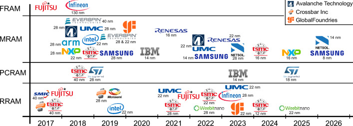
This prospective and performance summary provides a view on the state of the art of emerging non-volatile memory (eNVM) in the semiconductor industry. The overarching aim is to inform academic researchers of the status of these technologies in industry, so as to help direct the right academic research questions for future materials and device development. eNVM already have a strong foothold in the semiconductor industry with the main target of replacing embedded flash memory, and soon possibly DRAM and SRAM, i.e. replacing conventional memory. Magnetic and resistive memory are the current frontrunners among eNVM for embedded flash replacement and they are very advanced in this, which poses high demands on future academic research for eNVM for this purpose. Phase-change and ferroelectric memory are less available as commercially available products. The use of eNVM for new forms of artificial intelligence hardware is a much more open field for future academic research.
Keywords: Artificial intelligence; Electronic material; Emergent phenomena; Ferroelectric; Nanoelectronics; Neuromorphic; Spintronic; Thin film.
© The Author(s) 2024.
Conflict of interest statement
Conflict of interestThe authors declare no conflict of interest.
Figures
References
-
- Z. Wang et al., Advances of embedded resistive random access memory in industrial manufacturing and its potential applications. Int. J. Extrem. Manuf. 6(3), 032006 (2024). 10.1088/2631-7990/ad2fea - DOI
-
- Y. Chen, ReRAM: history, status, and future. IEEE Trans. Electron Devices 67(4), 1420–1433 (2020). 10.1109/TED.2019.2961505 - DOI
-
- M. Lanza, G. Molas, I. Naveh, The gap between academia and industry in resistive switching research. Nat. Electron. 6(4), 4 (2023). 10.1038/s41928-023-00954-8 - DOI
-
- M.J. Marinella, Radiation effects in advanced and emerging nonvolatile memories. IEEE Trans. Nucl. Sci. 68(5), 546–572 (2021). 10.1109/TNS.2021.3074139 - DOI
-
- J. Choi, SK hynix leads with “6th generation 10 nm” DRAM production ahead of Samsung (Businesskorea), https://www.businesskorea.co.kr/news/articleView.html?idxno=214703. Accessed 05 Aug 2024
Publication types
LinkOut - more resources
Full Text Sources