Indium aluminum nitride: A review on growth, properties, and applications in photovoltaic solar cells
- PMID: 39650183
- PMCID: PMC11625129
- DOI: 10.1016/j.heliyon.2024.e40322
Indium aluminum nitride: A review on growth, properties, and applications in photovoltaic solar cells
Abstract
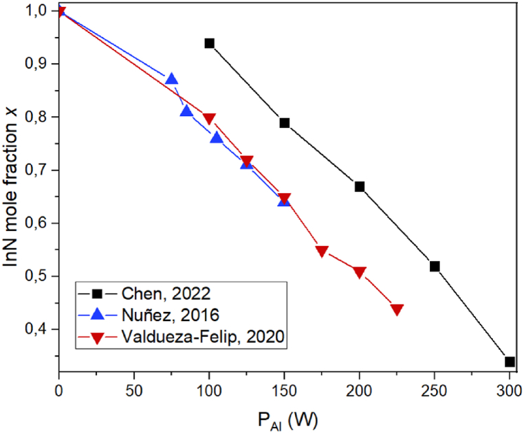
InAlN semiconductor alloy is a promising option for the fabrication of optoelectronic devices, such as high efficiency solar cells, due to its wide variable bandgap, from 0.64 eV to 6.2 eV. Traditionally, the production of high quality InAlN has been achieved by techniques such as MBE (Molecular Beam Epitaxy) and MOCVD (Chemical Vapor Deposition), which are complex and require high energy consumption. In contrast, sputtering is presented as a simpler, cheaper, and more industrially scalable technique, allowing the production of InAlN thin films with good structural quality. This study investigates the physical properties of InAlN layers to evaluate their potential in photovoltaic applications. Recent advances and challenges in the use of InAlN as an absorber layer in solar cells are discussed. In addition, critical parameters of the sputtering process, including target power, working pressure, gas flow ratio, substrate temperature, source type and number of cathodes and their influence on material properties are explored. These conditions are discussed along with their impact on the quality of InAlN thin films to enhance their application in photovoltaics and other emerging technology areas.
Keywords: Electrical properties; InxAl1-xN; Magnetron sputtering; Optical properties; Solar cells; Structural properties.
© 2024 Published by Elsevier Ltd.
Conflict of interest statement
The authors declare that they have no known competing financial interests or personal relationships that could have appeared to influence the work reported in this paper.
Figures


References
-
- Kubota K., Kobayashi Y., Fujimoto K., Kobayashi Y., Fujimoto K. Preparation and properties of III-V nitride thin films. J. Appl. Phys. 1989;2984 doi: 10.1063/1.344181. - DOI
-
- Yeh T.S., Wu J.M., Lan W.H. Electrical properties and optical bandgaps of AlInN films by reactive sputtering. J. Cryst. Growth. 2008;310(24):5308–5311. doi: 10.1016/j.jcrysgro.2008.09.166. - DOI
-
- Guo Q.X.Ã., Okazaki Y., Kume Y., Tanaka T., Nishio M., Ogawa H. Reactive sputter deposition of AlInN thin films. J. Cryst. Growth. 2007;300:151–154. doi: 10.1016/j.jcrysgro.2006.11.007. - DOI
-
- Afzal N., Devarajan M., Ibrahim K. Deposition and characterization of magnetron co-sputtered in AlN film at different Ar:N2 gas flow ratios. Surf. Rev. Lett. Apr. 2017;24(3) doi: 10.1142/S0218625X17500275. - DOI
-
- Zeng H., et al. Interface-engineered InAlN/Cu2O photocathode with accelerated charge separation for boosting photoelectrochemical water splitting. Sol. RRL. May 2024;8(10) doi: 10.1002/solr.202400094. - DOI
Publication types
LinkOut - more resources
Full Text Sources