. 2024 Dec 25;24(51):16231-16238.
doi: 10.1021/acs.nanolett.4c03574. Epub 2024 Dec 13.

Nanoscale Ferroelectric Programming of van der Waals Heterostructures

Affiliations

Nanoscale Ferroelectric Programming of van der Waals Heterostructures

Dengyu Yang et al. Nano Lett. .

Abstract

We demonstrate an approach to creating nanoscale potentials in van der Waals layers integrated with a buried programmable ferroelectric layer. Using ultra-low-voltage electron beam lithography (ULV-EBL), we can program the ferroelectric polarization in Al1-xBxN (AlBN) thin films, generating structures with sizes as small as 35 nm. We demonstrate the ferroelectric field effect with a graphene/vdW stack on AlBN by creating a p-n junction. This resist-free, high-resolution, contactless patterning method offers a new pathway to integrate ferroelectric films with a wide range of two-dimensional layers including transition-metal dichalcogenides (TMD), enabling arbitrary programming and top-down creation of multifunctional devices.

Keywords: ferroelectric; heterostructures; nanoscale potentials; van der Waals.


Conflict of interest statement

The authors declare no competing financial interest.

Figures

Figure 1
Figure 1
Ferroelectric switching using ULV-EBL. (a) Illustration of the vdW stack (hBN/graphene/hBN). (b) ULV-EBL programming of ferroelectric domains in AlBN grown on W/Al2O3. (c) Atomic structure of the wurtzite Al(B)N of N-polar and Al-polar cases. (d) Illustration of ferroelectric polarization patterning with ULV-EBL, through the vdW layer. (e) Monte Carlo simulation for electron trajectories of electron beam acceleration voltage Vacc = 2 kV at a graphene/hBN (10 nm) stack on 20 nm AlBN film. (f) AFM AC phase image of the ULV-EBL-exposed AlBN with a letter “P”. The scale bar represents 4 μm.
Figure 2
Figure 2
Characterization of AlBN ferroelectric and ULV-EBL patterned domains. (a) Positive-up and negative-down (PUND) measurements with applied voltage U and measured current I with respect to time. Four voltage pulses U with maximum and minimum +17 V and −17 V are applied across 20 nm AlBN through metal pads making contacts on top and below AlBN. The current I is measured in between the metal pads. (b) Current measured with 17 V PUND voltage pulses. The current differences in between P (or N) and U (or D) is the current that is coming from the polarization switching. (c) AFM height scan of four square rings with different electron-beam doses, after a KOH etching of 30 s. The red box is exposed with an area dose D1 = 51,200 μC/cm2. The green boxes are exposed with an area dose D2 = 25,600 μC/cm2. The blue box is exposed with an area dose D3 = 12,800 μC/cm2. The scale bar denotes 10 μm. (d) AFM topography after etching with KOH for 60 s. The upper is the AFM height image for the partial red region in (c). The lower is a line cut along the red line in the upper image for its height profile. The measured etch depth is 20 nm, which is the total AlBN thickness.
Figure 3
Figure 3
ULV-EBL ferroelectric switching resolution. (a) AFM phase image of a series of lines patterned with different doses. Lines D1, D2, D3, and D4 are exposed with doses of 100, 200, 400, and 800 pC/cm, respectively. The lower graph is a line cut of the upper image. (b) Line width w collected from lines in (a) with respect to their exposure dose D. (c) PFM phase image of a square lattice with dose gradient ranging linearly from 0.01 pC (top left) to 4 pC (bottom right) with 0.01 pC per step per dot.
Figure 4
Figure 4
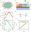
ULV-EBL ferroelectric switching on graphene. (a) Schematic diagram of the device. The blue region denotes the graphene/hBN device. There are electrical contacts to the graphene (yellow rectangles). The region enclosed by a dashed line is the ULV-EBL exposure region (transparent green color). The rest of the Hall bar is the no exposure region. (b) Schematic diagram of the device geometry. A monolayer graphene and 10 nm thick hBN vdW stack is placed on top of an AlBN/W/sapphire substrate. The AlBN is as-grown polarization-down state (orange region). The electron beam exposed region has polarization pointing up (green region). Different polarization induces different types of doping carriers in graphene, shown as electrons (blue circle) and holes (red circle). (c, d) RVg measurement before (light color line) and after (opaque line) the exposure to show the Dirac point for the unexposed (Ru) and exposed (Re) region. The blue dotted line denotes the original Dirac point position, and the blue arrow shows the direction of the shift. T = 300 K. (e) Illustration of the p–n junction energy band. Dashed line shows the Fermi energy, EF. (f) IV curves for the p–n junction and the unexposed region as a comparison. T = 15 mK.

References

    1. Yang D.; Hao S.; Chen J.; Guo Q.; Yu M.; Hu Y.; Eom K.; Lee J.-W.; Eom C.-B.; Irvin P.; Levy J. Nanoscale control of LaAlO3/SrTiO3 metal–insulator transition using ultra-low-voltage electron-beam lithography. Appl. Phys. Lett. 2020, 117, 253103.10.1063/5.0027480. - DOI
    1. Geim A. K.; Grigorieva I. V. Van der Waals heterostructures. Nature 2013, 499, 419–425. 10.1038/nature12385. - DOI - PubMed
    1. Cao Y.; Fatemi V.; Fang S.; Watanabe K.; Taniguchi T.; Kaxiras E.; Jarillo-Herrero P. Unconventional superconductivity in magic-angle graphene superlattices. Nature 2018, 556, 43–50. 10.1038/nature26160. - DOI - PubMed
    1. Yankowitz M.; Chen S.; Polshyn H.; Zhang Y.; Watanabe K.; Taniguchi T.; Graf D.; Young A. F.; Dean C. R. Tuning superconductivity in twisted bilayer graphene. Science 2019, 363, 1059–1064. 10.1126/science.aav1910. - DOI - PubMed
    1. Cao Y.; Fatemi V.; Demir A.; Fang S.; Tomarken S. L.; Luo J. Y.; Sanchez-Yamagishi J. D.; Watanabe K.; Taniguchi T.; Kaxiras E.; Ashoori R. C.; Jarillo-Herrero P. Correlated insulator behaviour at half-filling in magic-angle graphene superlattices. Nature 2018, 556, 80–84. 10.1038/nature26154. - DOI - PubMed

LinkOut - more resources