. 2025 Feb;12(6):e2410519.
doi: 10.1002/advs.202410519. Epub 2024 Dec 16.

Ternary Logic Transistors Using Multi-Stacked 2D Electron Gas Channels in Ultrathin Oxide Heterostructures

Affiliations

Ternary Logic Transistors Using Multi-Stacked 2D Electron Gas Channels in Ultrathin Oxide Heterostructures

Ji Hyeon Choi et al. Adv Sci (Weinh). 2025 Feb.

Abstract

2D electron gas field-effect transistors (2DEG-FETs), employing 2DEG formed at an interface of ultrathin (≈6 nm) Al2O3/ZnO heterostructure as the active channel, exhibit outstanding drive current (≈215 µA), subthreshold swing (≈132 mV dec-1), and field effect mobility (≈49.6 cm2 V-1 s-1) with a high on/off current ratio of ≈107. It is demonstrated that the Al2O3 upper layer in Al2O3/ZnO heterostructure acts as the source/drain resistance component during transistor operations, and the applied potential to the 2DEG channel is successfully modulated by Al2O3 thickness variations so that the threshold voltage (Vth) is effectively tuned. Remarkably, double-stacked 2DEG-FETs consisting of two Al2O3/ZnO heterostructured 2DEG channels with a single gate exhibit multiple Vth, enabling a ternary logic state in a single device. By inducing a voltage difference between the stacked channels, a sequential operation of the upper and lower FETs is achieved, successfully realizing a stable ternary logic operation.

Keywords: 2D electron gas; atomic layer deposition; multiple threshold voltage; multi‐stacked channel; ternary logic transistor.


Conflict of interest statement

The authors declare no conflict of interest.

Figures

Figure 1
Figure 1
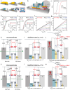
Electrical and physicochemical characteristics in Al2O3/ZnO 2DEG system. a) Rsh of Al2O3/ZnO heterostructures as a function of Al2O3 upper layer thickness on 5.5 nm‐thick ZnO lower layer. The results from epitaxial LAO/single crystal STO heterostructures, reproduced with permission,[ 24 ] Copyright 2010, Springer Nature, and our previous work of ALD‐grown Al2O3/TiO2 heterostructures, reproduced with permission,[ 23 ] Copyright 2018, American Chemical Society were also included for comparison. The Rsh decreased drastically at a specific thickness of each upper layer, implying the typical metal‐insulator transition in 2DEG system. b) Rsh of Al2O3/ZnO heterostructures as a function of ZnO lower layer thickness before and after Al2O3 deposition. c) A schematic of an in situ ALD process. d) An image of a specially designed in situ ALD reactor with integrated probe tips, enabling simultaneous electrical measurement during ALD process. e) Rsh of Al2O3/ZnO heterostructure measured in the in situ ALD reactor for every ALD Al2O3 full cycle; (precursor‐purge‐reactant‐purge) and f) for every ALD Al2O3 half cycle; (precursor‐purge)/(reactant‐purge). g) Normalized Zn 3d core‐level XPS spectra of bare ZnO and Al2O3/ZnO heterostructure. The spectra of Al2O3/ZnO exhibited a shift toward lower binding energy, indicating that reduction reaction occurs in ZnO during Al2O3 deposition. h) Cross‐sectional HRTEM image of Al2O3/ZnO heterostructure and i) corresponding HAADF image with EELS core‐loss spectra of O K‐edge and Zn L2,3 ‐edge at various positions along the direction perpendicular to the interface. j) EELS low‐loss spectra with estimated band gap at ZnO film (red line) and ZnO surface (blue line). k) Conductivity of Al2O3/ZnO heterostructure as a function of measurement temperature with calculated Vo donor level. l) Electronic band structure of Al2O3/ZnO heterostructure, showing generated electrons are confined to form 2DEG in quantum well, which is resulted from conduction‐band‐edge lowering effect due to overlapping of Vo donor states at the interface.
Figure 2
Figure 2
Operation mechanism of 2DEG‐FET. a) Fabrication procedure and b) a schematic of a top‐gated single‐stacked 2DEG‐FET using an ultrathin Al2O3/ZnO heterostructure. c) Normalized C‐V curves for single‐stacked 2DEG‐FETs with different Al2O3 layer thickness; 3 and 1.5 nm. Positive shift ≈1 V appears for thinner Al2O3 layer, indicating |1 V| less VGS is required to make 2DEG channel off. d) Transfer curves of single‐stacked 2DEG‐FETs with 3 nm‐thick and e) 1.5 nm‐thick Al2O3 layer. The extracted Vth for each device are −2.40 and −1.27 V, consistent with the roughly 1 V shift toward positive observed in the C–V curve for thinner Al2O3, demonstrating enhanced Vch due to lower VAl2O3 in thinner Al2O3 layer. f) Output curves of single‐stacked 2DEG‐FETs with 3 nm‐thick and g) 1.5 nm‐thick Al2O3 layer for every 0.5 V step of VGS. h) Electronic band structures of initial unconnected state, i) equilibrium state at VGS = 0 V, j) non‐equilibrium state with applied VGS, which induces potential drop of 0.82 eV in 2DEG channel for using 3 nm‐thick Al2O3 layer. k) Electronic band structures of initial unconnected state, l) equilibrium state at VGS = 0 V, m) non‐equilibrium state with applied VGS for using 1.5 nm‐thick Al2O3 layer, demonstrating |1 V| less VGS is required to make the electrical potential in 2DEG channel same with that for using 3 nm‐thick Al2O3 layer.
Figure 3
Figure 3
Ternary logic switching characteristics in double‐stacked 2DEG‐FETs. a) Cross‐sectional HRTEM image and EDS mapping of double‐stacked 2DEG heterostructures, displaying clear interface without intermixing layer. b) Schematics of double‐stacked 2DEG‐FETs, indicating three operating modes to realize ternary logic states depending on the VGS range. For on state, both 2DEG channels are all on; for intermediate state, only upper 2DEG channel is off but lower 2DEG channel is still on; for off state, both 2DEG channels are off. c) Transfer curves in linear scale of double‐stacked 2DEG‐FETs with 1 nm‐thick Al2O3 layer in the lower stack hardly achieve a stable intermediate state. d) Transfer curves with 1.5 nm‐thick Al2O3 layer in the lower stack show a slight intermediate state, indicating that the upper and lower 2DEG channels start to operate discretely at different VGS range, and therefore, two transfer curves are revealed. e) Transfer curves with 3 nm‐thick Al2O3 layer in the lower stack display an obvious intermediate state with two distinct transfer curves, indicating each 2DEG channel operates discretely and sequentially at differentVGS range, leading to the realization of ternary logic switching characteristics. The inset shows transconductance curve for VDS = 0.3 V. The yellow box indicates VGS range for the intermediate state; −6.5 to −4.5 V. f) VTC of a resistive‐load ternary NMOS inverter, consisting of double‐stacked 2DEG‐FETs with 3 nm‐thick Al2O3 layer in the lower stack and an external resistor, resulting in three distinct Vout; 2, 1.35, 0.86 V. The yellow box indicates VGS range for the intermediate state; −6.5 to −4.5 V. The inset shows the schematic diagram of the circuit for measurement.

References

    1. Zaitseva E., Levashenko V., Lukyanchuk I., Rabcan J., Kvassay M., Rusnak P., Electronics 2020, 9, 12.
    1. Heung A., Mouftah H. T., IEEE J. Solid‐State Circuits 1985, 20, 609.
    1. Yoeli M., Rosenfeld G., IEEE Transactions on Electronics Computer , IEEE; 1965, EC‐14, 19.
    1. Jo S. B., Kang J., Cho J. H., Adv. Sci. 2021, 8, 2004216. - PMC - PubMed
    1. Jung K. S., Heo K., Kim M. J., Andreev M., Seo S., Kim J. O., Lim J. H., Kim K. H., Kim S., Kim K. S., Adv. Sci. 2020, 7, 2000991. - PMC - PubMed

LinkOut - more resources