Optical sensors based on plasmonic nano-structures: A review
- PMID: 39720038
- PMCID: PMC11667642
- DOI: 10.1016/j.heliyon.2024.e40923
Optical sensors based on plasmonic nano-structures: A review
Abstract
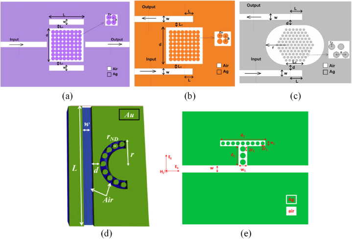
Optical sensors are among the most significant optical devices that have found extensive applications for THz sensing. Surface plasmon-based sensors have attracted increasing attention more than other kinds of optical sensors such as photonic crystal, optical fiber, and graphene sensors, owing to their compact footprint, fast reaction, and high sensitivity value. Therefore, this work reviews plasmonic sensor structures divided into three general categories. These category types are plasmonic sensors based on conventional basic platforms, coupled resonator structures, and periodic structures. Furthermore, periodic structures include two sub-categories named metal-insulator and insulator-insulator periodic structures. The most prevalent methods used to investigate such sensors are the finite element method (FEM) and finite-difference time-domain (FDTD) method. Also, the metal and insulator materials used are usually silver, gold, air, Si, SiO2, and so on. Based on the noted features, such sensors have obtained specific attention for many applications in chemistry, physics, and biomedical.
Keywords: Metal-insulator-metal waveguide; Optical; Sensitive sensor; Surface plamon polaritons; Tunable sensor; plasmonic sensor.
© 2024 The Authors.
Conflict of interest statement
The authors declare that they have no known competing financial interests or personal relationships that could have appeared to influence the work reported in this paper.
Figures


References
-
- Cherik I.C., Mohammadi S. Vertical tunneling field-effect transistor with germanium source and T-shaped silicon channel for switching and biosensing applications: a simulation study. IEEE Trans. Electron. Dev. 2022;69(9):5170–5176.
-
- Khani S., Hayati M. Compact microstrip lowpass filter with wide stopband and sharp roll-off. Microw. J. 2017;60(11):86–92.
-
- Cherik I.C., Mohammadi S. Dielectric modulated doping-less tunnel field-effect transistor, a novel biosensor based on cladding layer concept. IEEE Sensor. J. 2022;22(11):10308–10314.
-
- Khani S., Makki S.V.A.D., Mousavi S.M.H., Danaie M., Rezaei P. Adjustable compact dual-band microstrip bandpass filter using T-shaped resonators. Microw. Opt. Technol. Lett. 2017;59(12):2970–2975.
Publication types
LinkOut - more resources
Full Text Sources