

Numerical proceeding to calculate impurity states in 2D semiconductor heterostructures
- PMID: 39730546
- PMCID: PMC11680771
- DOI: 10.1038/s41598-024-81346-6
Numerical proceeding to calculate impurity states in 2D semiconductor heterostructures
Abstract
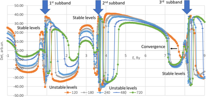
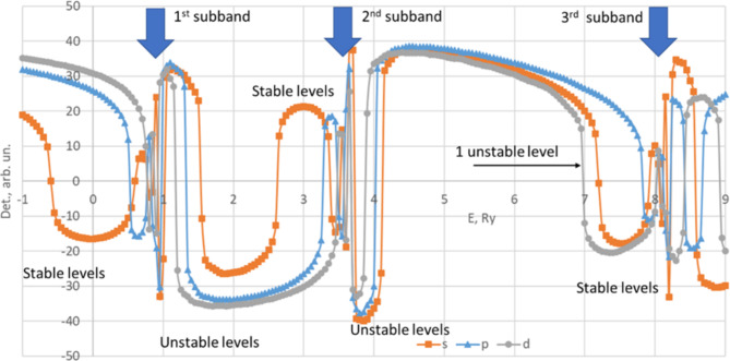
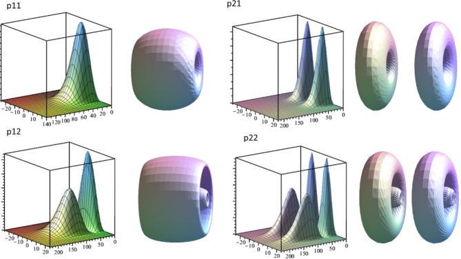
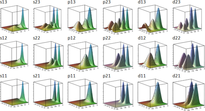
The article provides and discusses details of numerical proceeding for the expansion method to calculate energy positions and wave functions of the localized and resonant electronic states emerging in quantum well-type semiconductor nanostructures because of perturbation of confined states by the Coulomb potential of the hydrogenic impurity center. Effective mass approximation is used. Several excited both resonant and non-resonant states are calculated and classified for the case of a simple rectangular GaAs/AlGaAs quantum well. Results are compared to the ones in literature.
Keywords: Expansion method; Hydrogenic impurity states; Semiconductor heterostructures.
© 2024. The Author(s).
Conflict of interest statement
Declarations. Competing interests: The authors declare no competing interests.
Figures

References
-
- Chaves, A. et al. Bandgap engineering of two-dimensional semiconductor materials. npj 2D Mater. Appl.4, 29 (2020). - DOI
-
- Holmberg, V. C., Helps, J. R., Mkhoyan, K. A. & Norris, J. D. Imaging impurities in Semiconductor nanostructures. Chem. Mater.25, 8, 1332–1350 (2013). - DOI
-
- Tulupenko, V. et al. On the possibility of tuning the energy separation between space-quantized levels in a quantum well. Phil Mag Lett.93, 1, 42–49 (2012). - DOI
-
- Duque, C. A. et al. About possible THz modulator on the base of delta-doped QWs. Superlattice Microst. 87, 5–11 (2015). - DOI
LinkOut - more resources
Full Text Sources
