. 2025 Jan 2;16(1):291.
doi: 10.1038/s41467-024-54867-x.

Multiphase superconductivity in PdBi2

Affiliations

Multiphase superconductivity in PdBi2

Lewis Powell et al. Nat Commun. .

Abstract

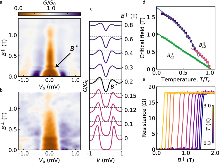
Unconventional superconductivity, where electron pairing does not involve electron-phonon interactions, is often attributed to magnetic correlations in a material. Well known examples include high-Tc cuprates and uranium-based heavy fermion superconductors. Less explored are unconventional superconductors with strong spin-orbit coupling, where interactions between spin-polarised electrons and external magnetic field can result in multiple superconducting phases and field-induced transitions between them, a rare phenomenon in the superconducting state. Here we report a magnetic-field driven phase transition in β-PdBi2, a layered non-magnetic superconductor. Our tunnelling spectroscopy on thin PdBi2 monocrystals incorporated in planar superconductor-insulator-normal metal junctions reveals a marked discontinuity in the superconducting properties with increasing in-plane field, which is consistent with a transition from conventional (s-wave) to nodal pairing. Our theoretical analysis suggests that this phase transition may arise from spin polarisation and spin-momentum locking caused by locally broken inversion symmetry, with p-wave pairing becoming energetically favourable in high fields. Our findings also reconcile earlier predictions of unconventional multigap superconductivity in β-PdBi2 with previous experiments where only a single s-wave gap could be detected.


Conflict of interest statement

Competing interests: The authors declare no competing interests.

Figures

Fig. 1
Fig. 1. Device design and tunnelling characteristics of β-PdBi2.
a Crystal structure of β-PdBi2. Bismuth atoms within each Bi-Pd-Bi layer are arranged tetragonally around Pd to form a square Bi bilayer. Neighbouring layers are staggered in an AB configuration. b Optical image of one of our devices. c Schematic of a device combining a tunnelling conductance measurement scheme (black) and four-probe contact configuration for resistance measurements (blue). For tunnelling, few-layer graphene (ball and stick model) acts as the normal metal, PdBi2 is the superconducting electrode (red), and 2-3 layer insulating hBN is used as a tunnel barrier (cyan). The entire structure is encapsulated in 100 nm hBN, not shown here. d Atomic-resolution cross-sectional STEM image of a thin slice lifted from a device after completing the tunnelling measurements (“Methods”). The inset shows a zoomed-in section of the main image overlapped with the simulated HAADF image (the latter outlined by the yellow dashed line). e Main panel: Temperature-dependent superconducting gap,Δ(T), extracted from fitting individual tunnelling spectra for device B (symbols). The dashed line is fit for weak-coupling BCS theory. Insets: Superconducting transition in R(T) (top) and a zero-field tunnelling conductance map (bottom). f Zero-field tunnelling spectra at different T, see labels. The spectra (black symbols) are accurately described by the standard Dynes model (solid blue lines). Data for device B. Source data are provided as a Source Data file.
Fig. 2
Fig. 2. Phase transition under in-plane magnetic field.
a, b Maps of the normalised tunnelling conductance for in-plane (a) and out-of-plane (b) magnetic fields. T=0.3 K. G0 corresponds to both electrodes being in the normal state. Brown areas correspond approximately to the spectral gap. The arrow in (a) indicates the transition field B* (see text). c Selected spectra from (a) emphasising the change in spectral shape at B*. Values of B are shown as labels. Dashed horizontal lines correspond to G/G0=0. d Temperature-dependent upper critical fields for in-plane and out-of-plane B extracted from R(B) measurements, such as shown in (e). Shown values of Bc2 correspond to R=0.9RN, where RN is the normal state resistance. Green circles showBc2, red squares Bc2 below the kink at 0.5 T, and blue squares Bc2 above 0.5 T. Solid lines are fits to Eqs. (4) and (5), see text. e Resistance vs in-plane magnetic field at different T. Data for device A. Source data are provided as a Source Data file.
Fig. 3
Fig. 3. Superconducting gap of PdBi2 for in-plane magnetic field.
a Main panel: Superconducting order parameter Δ extracted from fits to individual spectra vs in-plane magnetic field B. Data for device A (d 80 nm), T=0.3 K. Red squares correspond to Δ(B) extracted using the Maki theory and BCS DoS, dark-blue squares to nodal DoS (see text), and green squares are fit to the Maki theory in the intermediate region. The red solid line is fit for Eqs. (9, 10) yielding an apparent critical field for low-B s-wave superconductivity Bcswave0.25T. The Dashed blue line is a guide to the eye. Insets: Detailed view of Δ(B) in the low-B region for device A (top inset) and device B (bottom inset). A pronounced kink in Δ(B) seen for both devices, corresponds to suppression of the s-wave gap followed by the appearance of a new order parameter, as emphasised by the dashed lines (guides to the eye). b Representative spectra at B<B* (red squares) and B>B* (dark-blue squares) revealing the change from conventional (s-wave) to nodal gap. Solid lines are fits to the two models, see legend. Details of fitting are explained in Methods. c Evolution of the depairing strength parameter ζ(B∣∣) extracted from fitting of the experimental spectra to the Maki theory (blue symbols). Below B*, ζ follows the expected behaviour for an s-wave superconductor with a critical field Bcswave=0.25T;this is shown by the red solid line calculated using Eqs. (11), (12) (“Methods”). The dashed green line shows ζ(B∣∣) calculated using the same equations for an s-wave superconductor with Bc2=1.6T (actual upper critical field for our PdBi2). Attempting to apply the Maki theory above B* (as detailed in Supplementary Fig. 5b) results in unphysically large values of ζ; this is clear from a comparison between the extracted ζ (blue symbols) and the theory prediction (dashed green line). d Evolution of zero-bias conductance with B for device A (blue) and device B (red). For comparison, dashed lines show corresponding results predicted by theory (green) and experimental data for a conventional BCS superconductor (75 nm Sn film) taken from ref. (black). Source data are provided as a Source Data file.
Fig. 4
Fig. 4. Effect of the magnetic field on the free energy of s-wave and p-wave superconducting states of β-PdBi2 and the corresponding phase diagram.
a Normalised free energy at T=0.1Tc for several values of the magnetic field (colour-coded as indicated by dots in (b)) as a function of two possible order parameters: p-wave Δp in BCS units of Δ/1.76kBTc to the left of 0 (negative values) and s-wave Δs to the right. Within our model, p-wave pairing is insensitive to the magnetic field. Bottom-left inset: Isotropic lift of band degeneracy due to out-of-plane magnetic field. States of opposite momenta have opposite spin polarisations, favouring s-wave coupling. Top and bottom-right insets: Anisotropic lift of band degeneracy due to the in-plane magnetic field. States of opposite momenta, perpendicular to the direction of B, have parallel spin polarisation, favoring p-wave coupling. b Phase diagram constructed by minimising the free energy Fψ,η,B,T for the s-wave order parameter ψ and a spin-polarised triplet order parameter η. Transition to the nodal p-wave state occurs at a temperature-independent field B*. Coloured dots indicate the values of B corresponding to the free energy curves shown in (a). Source data are provided as a Source Data file.

References

    1. Leggett, A. J. A theoretical description of the new phases of liquid 3He. Rev. Mod. Phys.47, 331–414 (1975).
    1. Joynt, R. & Taillefer, L. The superconducting phases of UPt3. Rev. Mod. Phys.74, 235–294 (2002).
    1. Hayes, I. M. et al. Multicomponent superconducting order parameter in UTe2. Science373, 797–801 (2021). - PubMed
    1. Ott, H. R., Rudigier, H., Fisk, Z. & Smith, J. L. Phase transition in the superconducting state of U1-xThxBe13 (x=0–0.06). Phys. Rev. B31, 1651–1653 (1985). - PubMed
    1. Ran, S. et al. Nearly ferromagnetic spin-triplet superconductivity. Science365, 684–687 (2019). - PubMed

LinkOut - more resources