. 2025 Jan 3;14(1):30.
doi: 10.1038/s41377-024-01698-6.

From light sensing to adaptive learning: hafnium diselenide reconfigurable memcapacitive devices in neuromorphic computing

Affiliations

From light sensing to adaptive learning: hafnium diselenide reconfigurable memcapacitive devices in neuromorphic computing

Bashayr Alqahtani et al. Light Sci Appl. .

Abstract

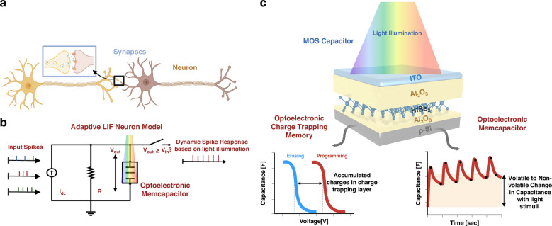
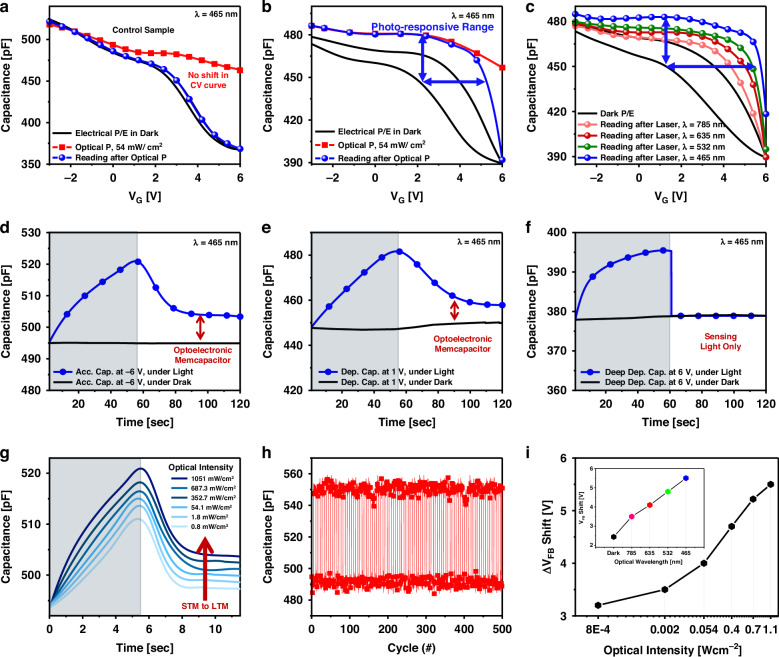
Advancements in neuromorphic computing have given an impetus to the development of systems with adaptive behavior, dynamic responses, and energy efficiency characteristics. Although charge-based or emerging memory technologies such as memristors have been developed to emulate synaptic plasticity, replicating the key functionality of neurons-integrating diverse presynaptic inputs to fire electrical impulses-has remained challenging. In this study, we developed reconfigurable metal-oxide-semiconductor capacitors (MOSCaps) based on hafnium diselenide (HfSe2). The proposed devices exhibit (1) optoelectronic synaptic features and perform separate stimulus-associated learning, indicating considerable adaptive neuron emulation, (2) dual light-enabled charge-trapping and memcapacitive behavior within the same MOSCap device, whose threshold voltage and capacitance vary based on the light intensity across the visible spectrum, (3) memcapacitor volatility tuning based on the biasing conditions, enabling the transition from volatile light sensing to non-volatile optical data retention. The reconfigurability and multifunctionality of MOSCap were used to integrate the device into a leaky integrate-and-fire neuron model within a spiking neural network to dynamically adjust firing patterns based on light stimuli and detect exoplanets through variations in light intensity.


Conflict of interest statement

Conflict of interest: The authors declare no competing interests.

Figures

Fig. 1
Fig. 1
Neuromorphic systems based on the structure of biological neurons. a Biological neurons interweave via synapses through synaptic chemical messengers, which are transmitted between presynaptic and post-synaptic neurons. b The charge-trapping MOS capacitor consists of multiple layers stacked on top of a silicon substrate. Under illumination, this device exhibits non-volatile charge trapping as well as a change in capacitance (i.e., memcapacitor). c The adaptive LIF neuron model consists of the input spikes represented as a current source, a leaky resistor, and the optoelectronic memcapacitor device. The light-modulated memcapacitor affects the neuron’s adaptability and the generated output spikes
Fig. 2
Fig. 2
HfSe2 flake characterization. a Atomic force microscopy scan of the nanosheets. b XRD peaks related to the flakes are highlighted in red. c Raman spectrum displaying the HfSe2 peak at (199 cm−1). d XPS spectra of Hf 4f for HfSe2. e XPS spectra of Se 3d for HfSe2. f EDX results confirming the material composition. g HRTEM of the cross-sectional images confirming the flakes’ material. Scale bar: 50 nm
Fig. 3
Fig. 3
Device’s electrical performance. a CV measurement of the control sample (without CTL) showing negligible memory window at ±6 V. b CV measurement of the device based on 2D material as CTL represents the shift in VFB of the P/E cycle at different biasing from ±4 to ±10 V. (inset: optical microscope image of the device under electrical propping). c Increment in the memory window with the increase in the basing voltage. d Charge tunneling analysis at different temperatures. The primary mechanism responsible for electron emission across the tunnel oxide is F–N tunneling, as indicated by the linear trend at high electric fields. e Cycle-to-cycle variability of MOS memory with a standard deviation of 0.028/0.031 of VFB shift for P/E cycles, receptively. f Device-to-device variability with a standard deviation of 0.14/0.10 of VFB shift for P/E cycles on different devices, receptively. g Endurance test revealed the memory window reliability after 104 P/E cycles. h Temperature-accelerated retention test reveals the device’s performance at 60 °C, 80 °C, and 100 °C temperatures. The device exhibits excellent memory stability when subjected to stressing temperatures of 60 °C and 80 °C. i Arrhenius (1/kT) plot extrapolation allows the estimation of the temperature at which the device can operate with memory stability above the threshold for 10 years
Fig. 4
Fig. 4
Optical characterization of the device. a The control sample showed no change after illumination. b The MOS capacitor based on 2D material CTL exhibited non-volatile optical data storage represented by the horizontal shift in the VFB of the reading curve after optical programming. The upward vertical CV curve shift indicates the memcapacitance mechanism. c Different VFB shifts were observed in response to various incident light wavelengths. The devices exhibited an 80% window enhancement through blue laser programming at the wavelength of 465 nm from 2 to 3.6 V at ±6 V bias. d CT measurement reveals the memcapacitance with the illumination in the accumulation region at −6 V biasing confirming optical data sensing and retention. e CT measurement showing a non-volatile change in capacitance with the illumination in the depletion region at 1 V biasing. f Deep depletion CT measurement exhibiting volatile light sensing at 6 V biasing. g MOS memory CT measurement clarifies the transition from STM to LTM based on optical programming intensity. h Memcapacitance device endurance under 500 cycles of optical programming (λ = 465 nm/12 mWcm2) in the accumulation region. i Memory window enhancement with optical programming intensity (inset: memory window based on the illumination wavelength)
Fig. 5
Fig. 5
Capacitive synaptic behavior. a Optical/electrical pulses are used for potentiation, whereas electrical pulses are used for depression. b Device exhibited a range of light-induced LTP in response to distinct illumination intensities. c LTD was observed based on electrical erasing signals from 6 to 8.5 V with a step of 0.5 V. d Capacitive synaptic weights change based on LTP/LTD. e The schematic of the capacitive synaptic array circuit. f The accuracy variation of handwritten digit recognition is higher than 96% at 20 epochs
Fig. 6
Fig. 6
Associated learning with memcapacitor. a An illustration of the control sample (without CTL) behavior under illumination, presenting various MOSCap regions. b Optoelectronic memcapacitor exhibited modulated light sensing based on the MOSCap region. c The learning process involves stimuli association, which strengthens synapses and enhances responses. Negative reinforcement occurs on association removal. d When testing a device with a red laser (λ = 635 nm) in the accumulation region, its memcapacitive response improved on being influenced by a blue laser (λ = 465 nm) due to associated learning. However, when the association was removed, the response of the device to the red laser gradually decreased over time (while illumination and in the dark) until it reached its previous level. The improvement was temporary and dependent on associated learning
Fig. 7
Fig. 7
Adaptive LIF Neuron and exoplanet detection. a A certain spike frequency is generated by the LIF neuron from the other neurons’ input with varying spike frequencies. The memcapacitor’s electrical and optical programming implies the neuron can dynamically adjust its response qualities. b During the CT measurement under varying light intensity (465 nm), the capacitance values of the memcapacitor alter considerably achieving eight levels. c The results of the simulation demonstrate that the light-modulated memcapacitor exhibits an adaptive behavior. The increased capacitance values reduce the output spikes when the device is illuminated (465 nm, 54.1 mWcm−2). The higher capacitance values cause the charging and discharging time to slow down, resulting in fewer spikes. d The transit method exhibits periodic fluctuations in a star’s brightness caused by an orbiting exoplanet crossing in front of it. e Dynamic illumination sensing neuron in the SNN for exoplanet detection. Each neuron receives input signals from a target star’s temporal light intensity variations. f The testing accuracy over increased epochs reached 90%

References

    1. Mead, C. Neuromorphic electronic systems. Proc. IEEE78, 1629–1636 (1990).
    1. Pakkenberg, B. & Gundersen, H. J. G. Neocortical neuron number in humans: effect of sex and age. J. Comp. Neurol.384, 312–320 (1997). - PubMed
    1. Yu, S. M. et al. Nonvolatile capacitive synapse: device candidates for charge domain compute-in-memory. IEEE Electron Devices Mag.1, 23–32 (2023).
    1. Zheng, Q. L. et al. Artificial neural network based on doped HfO2 ferroelectric capacitors with multilevel characteristics. IEEE Electron Device Lett.40, 1309–1312 (2019).
    1. Hur, J. et al. Nonvolatile capacitive crossbar array for in-memory computing. Adv. Intell. Syst.4, 2100258 (2022).

LinkOut - more resources