

Dramatic switchable polarities in conduction type and self-driven photocurrent of BiI3 via pressure engineering
- PMID: 39764507
- PMCID: PMC11702651
- DOI: 10.1093/nsr/nwae419
Dramatic switchable polarities in conduction type and self-driven photocurrent of BiI3 via pressure engineering
Abstract
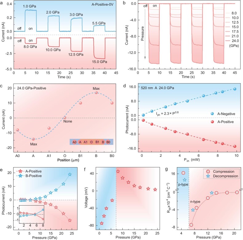
The intentional manipulation of carrier characteristics serves as a fundamental principle underlying various energy-related and optoelectronic semiconductor technologies. However, achieving switchable and reversible control of the polarity within a single material to design optimized devices remains a significant challenge. Herein, we successfully achieved dramatic reversible p-n switching during the semiconductor‒semiconductor phase transition in BiI3 via pressure, accompanied by a substantial improvement in their photoelectric properties. Carrier polarity flipping was monitored by measuring the photocurrent dominated by the photothermoelectric (PTE) effect in a zero-bias two-terminal device. Accompanying the p-n transition, a switch between positive and negative photocurrents was observed in BiI3, providing a feasible method to determine the conduction type of materials via photoelectric measurements. Furthermore, the combined effects of the photoconductivity and PTE mechanism improved the photoresponse and extended the detection bandwidth to encompass the optical communication waveband (1650 nm) under an external bias. The remarkable photoelectric properties were attributed to the enhanced energy band dispersion and increased charge density of BiI3 under pressure. These findings highlight the effective and flexible modulation of carrier properties through pressure engineering and provide a foundation for designing and implementing multifunctional logic circuits and optoelectronic devices.
Keywords: conduction-type switching; high pressure; metal halide; self-driven photocurrent.
© The Author(s) 2024. Published by Oxford University Press on behalf of China Science Publishing & Media Ltd.
Figures


Similar articles
-
Pressure-Tailored Self-Driven and Broadband Photoresponse in PbI2.Small Methods. 2022 Dec;6(12):e2201044. doi: 10.1002/smtd.202201044. Epub 2022 Nov 9. Small Methods. 2022. PMID: 36351755
-
Radical n-p Conduction Switching and Significant Photoconductivity Enhancement in NbOI2 via Pressure-Modulated Peierls Distortion.J Am Chem Soc. 2024 Sep 11;146(36):25245-25252. doi: 10.1021/jacs.4c09361. Epub 2024 Aug 28. J Am Chem Soc. 2024. PMID: 39196912
-
Pressure-Driven Reversible Switching between n- and p-Type Conduction in Chalcopyrite CuFeS2.J Am Chem Soc. 2019 Jan 9;141(1):505-510. doi: 10.1021/jacs.8b11269. Epub 2018 Dec 6. J Am Chem Soc. 2019. PMID: 30484644
-
Spontaneous Polarity Flipping in a 2D Heterobilayer Induced by Fluctuating Interfacial Carrier Flows.Nano Lett. 2021 Aug 25;21(16):6773-6780. doi: 10.1021/acs.nanolett.1c01356. Epub 2021 Aug 12. Nano Lett. 2021. PMID: 34382814
-
Synthesis of 2D Layered BiI3 Nanoplates, BiI3 /WSe2 van der Waals Heterostructures and Their Electronic, Optoelectronic Properties.Small. 2017 Oct;13(38). doi: 10.1002/smll.201701034. Epub 2017 Aug 9. Small. 2017. PMID: 28791794
Cited by
-
Pressure-induced p-n conductivity type switching and self-driven photocurrent polarity reversal in BiI3.Natl Sci Rev. 2025 May 29;12(7):nwaf192. doi: 10.1093/nsr/nwaf192. eCollection 2025 Jul. Natl Sci Rev. 2025. PMID: 40575719 Free PMC article. No abstract available.
References
-
- Euvrard J, Yan Y, Mitzi DB. Electrical doping in halide perovskites. Nat Rev Mater 2021; 6: 531–49.10.1038/s41578-021-00286-z - DOI
LinkOut - more resources
Full Text Sources