Review
. 2024 Dec 24;18(1):12.
doi: 10.3390/ma18010012.

The Overview of Silicon Carbide Technology: Status, Challenges, Key Drivers, and Product Roadmap

Affiliations
Review

The Overview of Silicon Carbide Technology: Status, Challenges, Key Drivers, and Product Roadmap

Maciej Kamiński et al. Materials (Basel). .

Abstract

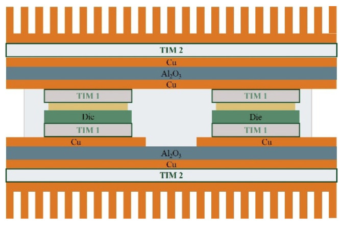
Arguably, SiC technology is the most rapidly expanding IC manufacturing technology driven mostly by the aggressive roadmap for battery electric vehicle penetration and also industrial high-voltage/high-power applications. This paper provides a comprehensive overview of the state of the art of SiC technology focusing on the challenges starting from the difficult and lengthy SiC substrate growth all the way to the complex MOSFET assembly processes. We focus on the differentiation from the established Si manufacturing processes and provide a comprehensive list of references as well as a brief description of our own research into the key manufacturing processes in this technology. We also present a SiC technology and product roadmap.

Keywords: SiC MOSFET; SiC technology; automotive industry; battery electric vehicles.


Conflict of interest statement

Andrzej Strójwąs was employed by the PDF Solutions, Inc. The remaining authors declare that the research was conducted in the absence of any commercial or financial relationships that could be construed as a potential conflict of interest.

Figures

Figure 1
Figure 1
An example of the SiC MOSFET manufacturing process flow.
Figure 2
Figure 2
Epitaxial layer growth.
Figure 3
Figure 3
SOITEC’s Smart Cut SiC wafer manufacturing process. Reproduced with permission from [5].
Figure 4
Figure 4
Activation ratio vs. temperature dependence (a) and resistivity of the region obtained during implantation at RT and at the elevated temperature (b). Reproduced with permission from [7].
Figure 5
Figure 5
Incomplete ionization ratio calculated using theoretical model at elevated temperatures (solid line) compared to parameterization of empirical data (dashed). Reprinted from [40], with permission from AIP Publishing.
Figure 6
Figure 6
Dependence between Vbr and implantation dose which was used for single-zone JTE fabrication. A dose of zero corresponds to the structures without JTE. Experimental points are shown as individual marks; the curves were obtained by simulation with various effective surface charges.
Figure 7
Figure 7
The 4H-SiC substrate with a SiO2 mask.
Figure 8
Figure 8
Selectivity of SiC etching over SiO2 in SF6 + O2 plasma as a function of (a) the plasma PRIE power at p = 30 mTorr and (b) the plasma pressure at PRIE = 250 W.
Figure 9
Figure 9
SEM image of the MESA structure obtained in the course of the RIE of 4H-SiC (at PRIE—300 W; O2 flowrate—30 sccm; SF6 flowrate—20 sccm; and p—30 mTorr). The height of this MESA structure was around 1.35 µm.
Figure 10
Figure 10
SEM images of MESA structures obtained after the ICP-RIE of SiC with the Cr mask in the SF6 plasma (no micro-trenching effect on the MESA sidewall is visible) performed with an magnification of (a) 220× (b) 1000× (c) 7000×. The etching process parameters were SF6 flowrate = 100 sccm, PRIE = 50 W, PICP = 2500 W, p = 7 mTorr, and t = ~18.5 min (a time of the total Cr mask etching).
Figure 11
Figure 11
Images of the SiC surface after ICP-RIE processes with two different types of masks: (a) the aluminum mask and (b) the AZ 4562 photoresist.
Figure 12
Figure 12
SEM images of SiC MESA structures after the ICP-RIE of SiC with photoresist AZ 4562 mask, with various RIE powers: (a) 100 W, (b) 200 W, and (c) 300 W. The pressure in the reactor was 7 mTorr and the ICP power was 800 W. The gas flowrates: SF6—18 sccm; O2—9 sccm.
Figure 13
Figure 13
SEM images of SiC structures after the ICP-RIE of SiC with photoresist AZ 4562 mask, with various ICP powers: (a) 800 W and (b) 1300 W. The pressure in the reactor was 7 mTorr and the RIE power was 100 W. The gas flowrates: O2—9 sccm; SF6—18 sccm.
Figure 14
Figure 14
SiC trenches obtained after ICP-RIE in pure SF6 plasma (photos at the top; PICP = 2250 W, PRIE = 50 W, p = 7 mTorr, gas flowrate SF6 = 100 sccm) and in SF6 + 50% O2 (photos at the bottom; PICP = 2250 W, PRIE = 50 W, p = 7 mTorr, gas flowrates: SF6 = 50 sccm and O2 = 50 sccm). (a,d) View of the structure profile; (b,e) SiC surface morphology; (c,f) view of sidewalls with the inclination angles of ~90° and ~63°, respectively.
Figure 15
Figure 15
Typical energy distribution of trap state densities across the 4H-SiC bandgap for samples produced in dry oxidation.
Figure 16
Figure 16
Identified defects in the 4H-SiC–SiO2 interface contributing to the active trap profile: <1> without stacking fault and <2> with stacking fault. Based on [88,92,94].
Figure 17
Figure 17
Trap density profiles calculated by the Hi-Lo method (100 kHz) near the conduction band edge of 4H-SiC (0001). (a) Black diamonds—simple dry oxidation at 1175 °C; green triangles—a simple dry oxidation followed by the 1000 °C NO annealing step. (b) Black diamonds—simple dry oxidation at 1175 °C; brown squares—a simple dry oxidation followed by the POCl3 annealing and subsequent NO annealing step at 1000 °C; green triangles—a simple dry oxidation followed by the 1000 °C NO annealing step for comparison. Dashed lines—a fitted U-shaped profile (U6) for each sample. Based on [106].
Figure 18
Figure 18
Scheme of first-generation SiC power modules. TIM1 at chip—DBC interface; TIM2 at DBC—radiator interface.
Figure 19
Figure 19
Flex printed circuit board solution (SKIN).
Figure 20
Figure 20
Direct Lead Bonding (DLB) structure.
Figure 21
Figure 21
Package with double-sided cooling.

References

    1. SiC Wafer Size Trends. ST Microelectronics; Geneva, Switzerland: 2022.
    1. SiC Market Segment Size Growth Trends. Yole Report; Lyon, France: 2023.
    1. Langpoklakpam C., Liu A.-C., Chu K.-H., Hsu L.-H., Lee W.-C., Chen S.-C., Sun C.-W., Shih M.-H., Lee K.-Y., Kuo H.-C. Review of Silicon Carbide Processing for Power MOSFET. Crystals. 2022;12:245. doi: 10.3390/cryst12020245. - DOI
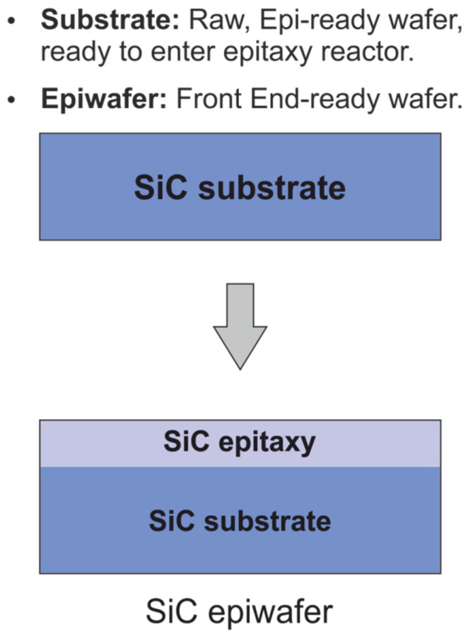
    1. Epitaxial layer growth; Proceedings of the SOITEC, Leti Workshop; San Francisco, CA, USA. 12 April 2022.
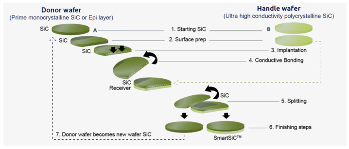
    1. SOITEC’s Smart Cut SiC wafer manufacturing process; Proceedings of the SOITEC, Leti Workshop; San Francisco, CA, USA. 12 April 2022.

LinkOut - more resources