

Highly bright perovskite light-emitting diodes enabled by retarded Auger recombination
- PMID: 39843419
- PMCID: PMC11754759
- DOI: 10.1038/s41467-025-56001-x
Highly bright perovskite light-emitting diodes enabled by retarded Auger recombination
Abstract
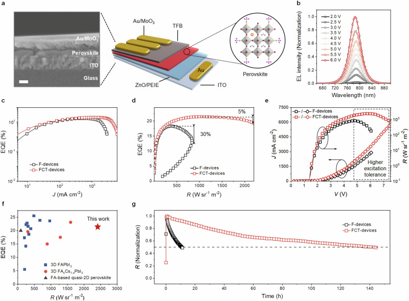
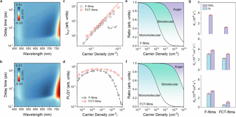
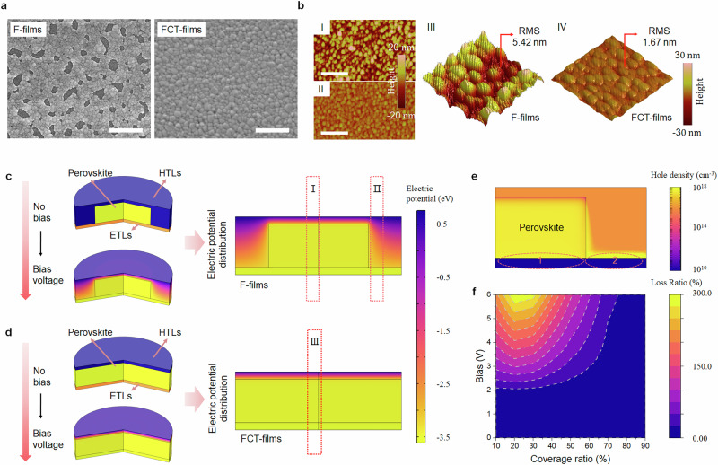
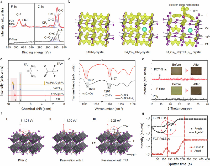
One of the key advantages of perovskite light-emitting diodes (PeLEDs) is their potential to achieve high performance at much higher current densities compared to conventional solution-processed emitters. However, state-of-the-art PeLEDs have not yet reached this potential, often suffering from severe current-efficiency roll-off under intensive electrical excitations. Here, we demonstrate bright PeLEDs, with a peak radiance of 2409 W sr-1 m-2 and negligible current-efficiency roll-off, maintaining high external quantum efficiency over 20% even at current densities as high as 2270 mA cm-2. This significant improvement is achieved through the incorporation of electron-withdrawing trifluoroacetate anions into three-dimensional perovskite emitters, resulting in retarded Auger recombination due to a decoupled electron-hole wavefunction. Trifluoroacetate anions can additionally alter the crystallization dynamics and inhibit halide migration, facilitating charge injection balance and improving the tolerance of perovskites under high voltages. Our findings shed light on a promising future for perovskite emitters in high-power light-emitting applications, including laser diodes.
© 2025. The Author(s).
Conflict of interest statement
Competing interests: The authors declare no competing interests.
Figures
Similar articles
-
Suppressing Efficiency Roll-Off at High Current Densities for Ultra-Bright Green Perovskite Light-Emitting Diodes.ACS Nano. 2020 May 26;14(5):6076-6086. doi: 10.1021/acsnano.0c01817. Epub 2020 Apr 28. ACS Nano. 2020. PMID: 32324379
-
High-Brightness Perovskite Light-Emitting Diodes with Suppressed Efficiency Roll-off Using the Green Solvent γ-Valerolactone.ACS Nano. 2025 Mar 11;19(9):9053-9060. doi: 10.1021/acsnano.4c17765. Epub 2025 Feb 26. ACS Nano. 2025. PMID: 40009790
-
Ultrabright Blue Lead-Halide Perovskite Light-Emitting Diodes Based on Phosphonic Acid Functionalized Hole Injection Layer.ACS Nano. 2025 May 6;19(17):16850-16858. doi: 10.1021/acsnano.5c01879. Epub 2025 Apr 21. ACS Nano. 2025. PMID: 40257445
-
Luminescence and Degeneration Mechanism of Perovskite Light-Emitting Diodes and Strategies for Improving Device Performance.Small Methods. 2023 Oct;7(10):e2300434. doi: 10.1002/smtd.202300434. Epub 2023 Jul 11. Small Methods. 2023. PMID: 37434048 Review.
-
Device Engineering for All-Inorganic Perovskite Light-Emitting Diodes.Nanomaterials (Basel). 2019 Jul 12;9(7):1007. doi: 10.3390/nano9071007. Nanomaterials (Basel). 2019. PMID: 31336905 Free PMC article. Review.
Cited by
-
Electron Extraction Optimization for Carbon-Based Hole-Conductor-Free Perovskite Photovoltaics With Record 1.41 V VOC.Adv Mater. 2025 Jul;37(26):e2502436. doi: 10.1002/adma.202502436. Epub 2025 Apr 16. Adv Mater. 2025. PMID: 40237209 Free PMC article.
-
Decoding the Role of Interface Engineering in Energy Transfer: Pathways to Enhanced Efficiency and Stability in Quasi-2D Perovskite Light-Emitting Diodes.Nanomaterials (Basel). 2025 Apr 12;15(8):592. doi: 10.3390/nano15080592. Nanomaterials (Basel). 2025. PMID: 40278458 Free PMC article. Review.
References
-
- Liu, X. et al. Metal halide perovskites for light-emitting diodes. Nat. Mater. 20, 10–21 (2021). - PubMed
-
- Xu, W. et al. Rational molecular passivation for high-performance perovskite light-emitting diodes. Nat. Photonics13, 418–424 (2019).
-
- Chen, J. et al. Efficient and bright white light-emitting diodes based on single-layer heterophase halide perovskites. Nat. Photon.15, 238–244 (2020).
-
- Tsai, H. et al. Bright and stable light-emitting diodes made with perovskite nanocrystals stabilized in metal–organic frameworks. Nat. Photon.15, 843–849 (2021).
LinkOut - more resources
Full Text Sources
Research Materials
