Review
. 2024 Dec 16;26(1):2436347.
doi: 10.1080/14686996.2024.2436347. eCollection 2025.

Integrating machine learning with advanced processing and characterization for polycrystalline materials: a methodology review and application to iron-based superconductors

Affiliations
Review

Integrating machine learning with advanced processing and characterization for polycrystalline materials: a methodology review and application to iron-based superconductors

Akiyasu Yamamoto et al. Sci Technol Adv Mater. .

Abstract

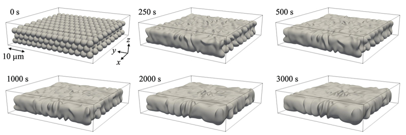
In this review, we present a new set of machine learning-based materials research methodologies for polycrystalline materials developed through the Core Research for Evolutionary Science and Technology project of the Japan Science and Technology Agency. We focus on the constituents of polycrystalline materials (i.e. grains, grain boundaries [GBs], and microstructures) and summarize their various aspects (experimental synthesis, artificial single GBs, multiscale experimental data acquisition via electron microscopy, formation process modeling, property description modeling, 3D reconstruction, and data-driven design methods). Specifically, we discuss a mechanochemical process involving high-energy milling, in situ observation of microstructural formation using 3D scanning transmission electron microscopy, phase-field modeling coupled with Bayesian data assimilation, nano-orientation analysis via scanning precession electron diffraction, semantic segmentation using neural network models, and the Bayesian-optimization-based process design using BOXVIA software. As a proof of concept, a researcher- and data-driven process design methodology is applied to a polycrystalline iron-based superconductor to evaluate its bulk magnet properties. Finally, future challenges and prospects for data-driven material development and iron-based superconductors are discussed.

Keywords: 3D reconstruction; 4D STEM; BOXVIA; Bayesian optimization; DFT; Iron-based superconductor; data assimilation; data-driven process design; deep learning; electron microscopy; fully convolutional neural networks; grain boundaries; high-energy milling process; machine learning; magnet; multiscale observation; phase-field modeling; polycrystalline materials; processing; researcher-driven process design; scanning precession electron diffraction; superconductor; thin films; trapped field.

Plain language summary

We present a new set of machine learning-based materials research methodologies for polycrystalline materials, such as a mechanochemical process involving high-energy milling, in situ observation of microstructural formation using 3D scanning transmission electron microscopy, phase-field modeling coupled with Bayesian data assimilation, nano-orientation analysis via scanning precession electron diffraction, semantic segmentation using neural network models, and the Bayesian-optimization-based process design using the BOXVIA software.


Conflict of interest statement

No potential conflict of interest was reported by the author(s).

Figures

None
Graphical abstract
Figure 1.
Figure 1.
Grain boundary (GB) properties of various iron-based superconductors. (a) Intergrain critical current density (Jc) of [001]-tilt GBs for (Ba,K)Fe2As2 [19], NdFeAs(O,F) [108], Ba(Fe,Co)2As2 [69], and Fe(Se,Te) [112] as function of GB angle. The measured reduced temperatures are shown in the panel. (b) Ratio of intergrain Jc (Jc,inter) to intragrain Jc (Jc,intra) as function of GB angle shown in (a). (c) Enlarged view of (b) at 0° θGB 16°. (d) Ratio of intergrain Jc to intragrain Jc of (Ba,K)Fe2As2 at 12 K. Applied magnetic fields of 1 and 5 T for H||c. For comparison, the data of Ba(Fe,Co)2As2 at 4 K are shown [69]. (e) Jc,inter/Jc,intra of FeSe0.5Te0.5 [010]-tilt GB as function of GB angle of FeSe0.5Te0.5 (θGBFST). For comparison, the data of Fe(Se,Te) for [001]-tilt GB at 4 and 4.2 K are superimposed [104,113].
Figure 2.
Figure 2.
Ball-milling energy (EBM) dependence of (a) magnetic superconducting transition temperature (Tcmag) and onset Tcmag (Tcmagonset) defined as the temperatures at which the magnetization reached 90% and 99.9% of the transition, respectively, resistive superconducting transition temperature (Tcres) determined based on the 90% of the superconducting transition, and zero-resistance temperature (Tcres0) of Ba(Fe,Co)2As2 bulk samples and (b) critical current density (Jc) at 5 K under self-field [106].
Figure 3.
Figure 3.
Sintering temperature dependence of density (left axis) and relative density to theoretical density (right axis) of (Ba,K)Fe2As2 bulk samples [79].
Figure 4.
Figure 4.
Mutiscale and multidimensional electron microscopy imaging platform for the present study.
Figure 5.
Figure 5.
Image in scanning electron microscopy in backscattered electron mode of Co-doped Ba122 bulk fabricated via self-sintering through mechanochemical process [230]. The inset shows a bright-field transmission electron microscopy image of neck area.
Figure 6.
Figure 6.
(a) High-angle annular dark-field scanning transmission electron microscopy (HAADF-STEM) image of planar defects in Ba122 bulk and (b) geometric phase analysis. The arrowheads in (b) indicate the strained area due to planar defects. (c)–(f) HAADF-STEM images of grain boundaries: (c) randomly oriented boundary, (d) boundary with amorphous phase, (e) small-misorientation-angle boundary, and (f) c-axis-oriented boundary.
Figure 7.
Figure 7.
(a) Bright-field scanning transmission electron microscopy image and inverse pole figure map acquired via transmission electron microscopy – scanning precession electron diffraction of Co-doped Ba122 bulk. (b) Misorientation angle of GBs obtained from grain orientation data of (a).
Figure 8.
Figure 8.
Correlation between Jc and inverse grain size for K-doped Ba122. Open symbols indicate data for randomly oriented bulks/wires [20,79,81,230,232] and closed symbols indicate data for uniaxially oriented tape wires [174,188,233–235]. Jc measurement conditions and grain size measurement methods are shown in each paper [20,38,79,81,174,188,230,232–235].
Figure 9.
Figure 9.
Specimen preparation/transfer/heating system for in situ heating with electron tomography observation of nanoparticles (NPs) [16]. (a) Sample preparation processes for transmission electron microscopy (TEM) observation (all performed in Ar-gas-filled glove box). (b) Sample carried by newly designed microelectromechanical system (mems) – based in situ heating holder with maintained air tightness. (c) Cu NPs dispersed on MEMS microheater. (d) Table and schematic diagram showing heating process in TEM. Because the MEMS holder can instantaneously increase or decrease the sample temperature, a tilt-series dataset can be acquired at a standby temperature (200°C) immediately after each heating step. (e) Temporal evolution of 3D morphology of Cu NPs during heating. The obtained data were averaged in the range of 3 × 3 × 3 pixels (30.4 nm3) for visibility. Reproduced from [16] with permission from the royal society of chemistry.
Figure 10.
Figure 10.
Modeling of 3D microstructures of actual materials via deep learning [17].
Figure 11.
Figure 11.
3D segmentation images of Ba-122 phase of the bulks fabricated with EBM of 80 MJ/kg (a) and 230 MJ/kg (b), and that of pore of the bulk EBM of 80 MJ/kg (c). The Jc obtained at 5 K under self-field and grain size of the bulk fabricated with EBM of 80 MJ/kg and 230 MJ/kg are 1.7 × 104 A/cm2 and 3. 7 × 103 A/cm2, 140 nm and 50 nm, respectively [15]. The example of method for measurement thickness of 3D-reconstructed image (d). (e) is schematic diagram of relationship between total pore length and local current.
Figure 12.
Figure 12.
Evolution of cost function calculated through DA using in situ observation data. The solid line shows the evolution of the cost function minimum updated during iterative minimization.
Figure 13.
Figure 13.
(a) Results of in situ observation of solid-state Cu nanoparticle sintering and (b) predictions obtained using phase-field simulation and optimally estimated parameters. The sintering time for each image (from left to right) are 0, 13.5, 31.5, and 45 s.
Figure 14.
Figure 14.
Schematic illustrations of Ba122: (a) unit cell, (b) (001) surface terminated by Ba layer (ba-t), and (c) (001) surface terminated by as layer (As-t) slab models. The green, orange, and purple balls represent Ba, Fe, and as atoms, respectively. The crystal structure of Ba122 consists of alternating Ba and FeAs layers in the [001] direction. These slab models have two equivalent surfaces and are nonstoichiometric.
Figure 15.
Figure 15.
Schematic illustration and top views of Ba122: (a) bulk model and (b) (001), (c) (100), (d) (110), and (e) (011) planes. The green, orange, and purple balls represent Ba, Fe, and as atoms, respectively. The terminated structures of the (001) plane are Ba-t and As-t, resulting from cleavage and the reconstructed 2×2 structure [270]. In the (100), (110), and (011) planes, only cleavage structures are considered. (i), (ii), and (iii) denote the different cleavage modes.
Figure 16.
Figure 16.
Slab models for (a) (001), (b) (100), (c) (110), and (d) (011) planes corresponding to Figure 15.
Figure 17.
Figure 17.
Anisotropy function of surface energy for Ba122 surfaces expressed by Equation (5). The anisotropy coefficients are k0s = 0.905, k1s = 0.358, k2s = 0.404, and k3s = 0.004.
Figure 18.
Figure 18.
Initial distributions of multi-Ba122 particles: (a) ρ = 0.5 isosurface, (b) surface energy distribution, and (c) crystal orientation (electron backscatter diffraction – inverse pole figure map) in z = 6.4 μm cross section. The Ba122 particles are in a hexagonal close-packed configuration, and the initial crystal orientations are assigned randomly.
Figure 19.
Figure 19.
Time evolutions of isosurface ρ = 0.5 obtained from phase-field simulation using multi-Ba122 particles.
Figure 20.
Figure 20.
Time evolutions of (a) crystal orientation (electron backscatter diffraction – inverse pole figure [IPF] map) in z = 6.4 μm cross section, and (b) distribution of area of grains in IPF color map obtained from phase-field simulation using multi-Ba122 particles.
Figure 21.
Figure 21.
Framework for researchers and artificial intelligence to design processes independently while sharing same experimental data [20].
Figure 22.
Figure 22.
Magnetic hysteresis loop of K-doped Ba122 bulk pair. The hysteresis loop was obtained by cooling the sample down to 5 K under a zero magnetic field, followed by a gradual increase in the external magnetic field from 0 T to 7 T, followed by a decrease from 7 T to − 7 T and another increase from − 7 T to 7 T (indicated by arrows) [20].

Similar articles

References

    1. Yamakoshi K, Ohno Y, Kutsukake K, et al. Multicrystalline informatics applied to multicrystalline silicon for unraveling the microscopic root cause of dislocation generation. Adv Mater. 2024;36(8):2308599. doi: 10.1002/adma.202308599 - DOI - PubMed
    1. Liu Y, Zhao T, Ju W, et al. Materials discovery and design using machine learning. J Materiomics. 2017;3(3):159–39. doi: 10.1016/j.jmat.2017.08.002 - DOI
    1. Mobarak MH, Mimona MA, Islam MA, et al. Scope of machine learning in materials research—a review. Appl Surf Sci Adv. 2023;18:100523. doi: 10.1016/j.apsadv.2023.100523 - DOI
    1. Ng WL, Goh GL, Goh GD, et al. Progress and opportunities for machine learning in materials and processes of additive manufacturing. Adv Mater. 2024;36(34):2310006. doi: 10.1002/adma.202310006 - DOI - PubMed
    1. Zhichao L, Dong M, Xiongjun L, et al. High-throughput and data-driven machine learning techniques for discovering high-entropy alloys. Commun Mater. 2024;5(1):76. doi: 10.1038/s43246-024-00487-3 - DOI

LinkOut - more resources