Recovery Analysis of Sequentially Irradiated and NBT-Stressed VDMOS Transistors
- PMID: 39858683
- PMCID: PMC11767675
- DOI: 10.3390/mi16010027
Recovery Analysis of Sequentially Irradiated and NBT-Stressed VDMOS Transistors
Abstract
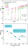
This study investigates the effects of negative bias temperature (NBT) stress and irradiation on the threshold voltage (VT) of p-channel VDMOS transistors, focusing on degradation, recovery after each type of stress, and operational behavior under varying conditions. Shifts in VT (ΔVT) were analyzed under different stress orders, showing distinct influence mechanisms, including defects creation and their removal and electrochemical reactions. Recovery data after each type of stress indicated ongoing electrochemical processes, influencing subsequent stress responses. Although the ΔVT is not particularly pronounced during the recovery after irradiation, changes in subthreshold characteristics indicate the changes in defect densities that affect the behavior of the components during further application. Additionally, the findings show that the ΔVT during the NBT stress after irradiation (up to certain doses and conditions) remains relatively stable, but this is the result of a balance of competing mechanisms. A subthreshold characteristic analysis provided a further insight into the degradation dynamics. A particular attention was paid to analyzing ΔVT with a focus on predicting the lifetime. In practical applications, especially under pulsed operation, prior stresses altered the device's thermal and electrical performance. It was shown that self-heating effects were more pronounced in pre-stressed components, increasing the power dissipation and thermal instability. These insights additionally highlight the importance of understanding stress-induced degradation and recovery mechanisms for optimizing VDMOS transistor reliability in advanced electronic systems.
Keywords: NBTI stress; VDMOS; irradiation; recovery; reliability; self-heating.
Conflict of interest statement
The authors declare no conflicts of interest.
Figures


References
-
- Mitrović N., Veljković S., Prijić Z., Danković D. Lifetime estimation of p-channel power VDMOSFETs applied in automotive applications; Proceedings of the IEEE Zooming Innovation in Consumer Technologies Conference (ZINC 2023); Novi Sad, Serbia. 29–31 May 2023; pp. 97–100.
-
- Veljković S., Mitrović N., Davidović V., Živanović E., Ristić G., Danković D. Successive Irradiation and Bias Temperature Stress Induced Effects on Commercial P-Channel Power VDMOS Transistors. FU Elec. Energ. 2024;37:561–579.
-
- Davidović V., Danković D., Golubović S., Djoric-Veljkovic S., Manić I., Prijić Z., Prijić A., Stojadinović N., Stanković S. NBT Stress and Radiation Related Degradation and Underlying Mechanisms in Power VDMOSFETS. FU Elec. Energ. 2018;31:367–388. doi: 10.2298/FUEE1803367D. - DOI
-
- Djorić-Veljković S., Manić I., Davidović V., Danković D., Golubović S., Stojadinović N. Annealing of Radiation-Induced Defects in Burn-in Stressed Power VDMOSFET. Nucl. Technol. Radiat. 2011;26:18–24. doi: 10.2298/NTRP1101018D. - DOI
-
- Sun Y., Wang T., Liu Z., Xu J. Investigation of irradiation effects and model parameter extraction for VDMOS field-effect transistor exposed to gamma rays. Radiat. Phys. Chem. 2021;185:109478. doi: 10.1016/j.radphyschem.2021.109478. - DOI
Grants and funding
LinkOut - more resources
Full Text Sources

