

The SPICE Modeling of a Radiation Sensor Based on a MOSFET with a Dielectric HfO2/SiO2 Double-Layer
- PMID: 39860914
- PMCID: PMC11769428
- DOI: 10.3390/s25020546
The SPICE Modeling of a Radiation Sensor Based on a MOSFET with a Dielectric HfO2/SiO2 Double-Layer
Abstract
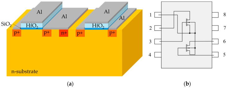
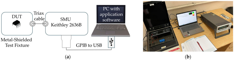
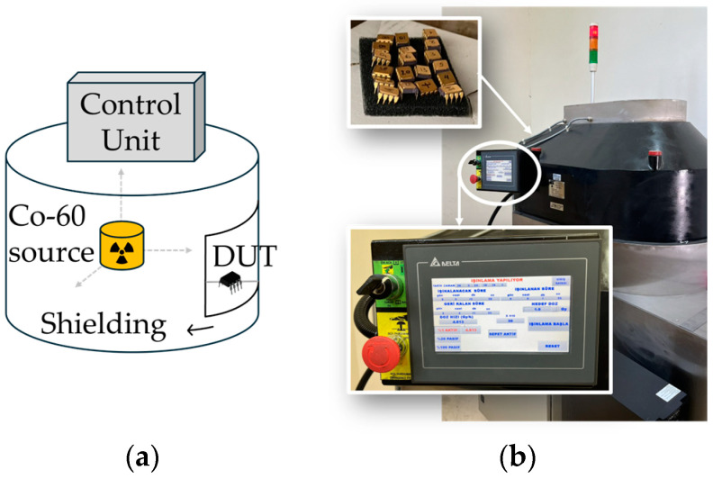
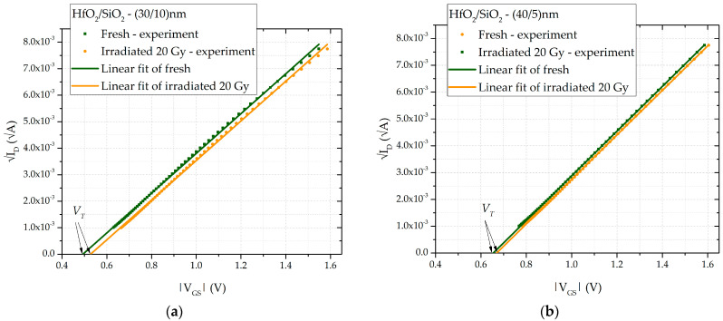
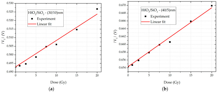
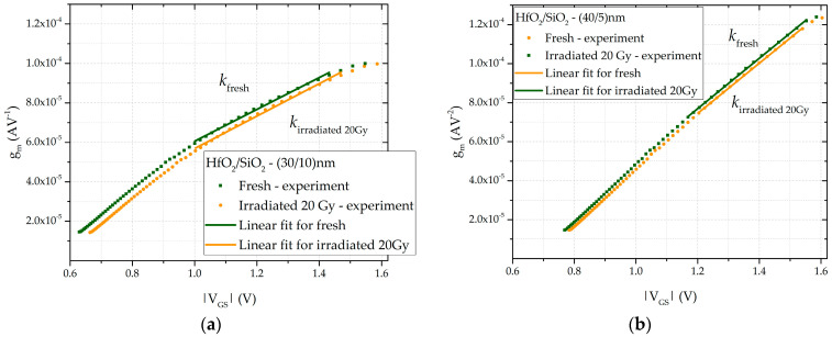
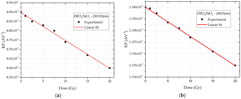
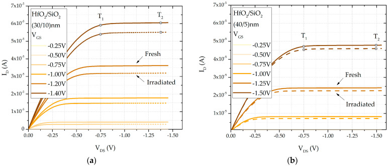
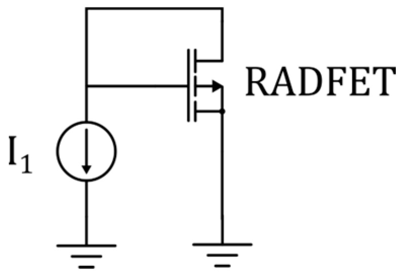
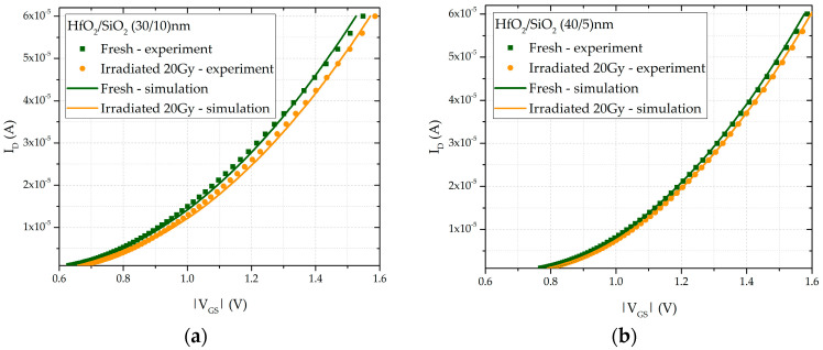
We report on a procedure for extracting the SPICE model parameters of a RADFET sensor with a dielectric HfO2/SiO2 double-layer. RADFETs, traditionally fabricated as PMOS transistors with SiO2, are enhanced by incorporating high-k dielectric materials such as HfO2 to reduce oxide thickness in modern radiation sensors. The fabrication steps of the sensor are outlined, and model parameters, including the threshold voltage and transconductance, are extracted based on experimental data. Experimental setups for measuring electrical characteristics and irradiation are described, and a method for determining model parameters dependent on the accumulated dose is provided. A SPICE model card is proposed, including parameters for two dielectric thicknesses: (30/10) nm and (40/5) nm. The sensitivities of the sensors are 1.685 mV/Gy and 0.78 mV/Gy, respectively. The model is calibrated for doses up to 20 Gy, and good agreement between experimental and simulation results validates the proposed model.
Keywords: RADFET; SPICE model; electrical simulation; high-k materials; radiation sensor.
Conflict of interest statement
The authors declare no conflicts of interest. The funders had no role in the design of the study; in the collection, analyses, or interpretation of data; in the writing of the manuscript; or in the decision to publish the results.
Figures
Similar articles
-
Dose response, radiation sensitivity and signal fading of p-channel MOSFETs (RADFETs) irradiated up to 50 Gy with ⁶⁰Co.Appl Radiat Isot. 2015 Oct;104:100-5. doi: 10.1016/j.apradiso.2015.06.024. Epub 2015 Jun 20. Appl Radiat Isot. 2015. PMID: 26142808
-
Effects of HfO2 encapsulation on electrical performances of few-layered MoS2 transistor with ALD HfO2 as back-gate dielectric.Nanotechnology. 2018 Aug 24;29(34):345201. doi: 10.1088/1361-6528/aac853. Epub 2018 May 29. Nanotechnology. 2018. PMID: 29808825
-
Investigation of RadFET response to X-ray and electron beams.Appl Radiat Isot. 2017 Sep;127:156-160. doi: 10.1016/j.apradiso.2017.06.004. Epub 2017 Jun 8. Appl Radiat Isot. 2017. PMID: 28622597
-
Electrical Properties of Ultrathin Hf-Ti-O Higher k Gate Dielectric Films and Their Application in ETSOI MOSFET.Nanoscale Res Lett. 2016 Dec;11(1):533. doi: 10.1186/s11671-016-1754-5. Epub 2016 Nov 30. Nanoscale Res Lett. 2016. PMID: 27905095 Free PMC article.
-
P-channel MOSFET as ionizing radiation detector.Appl Radiat Isot. 2023 Jun;196:110730. doi: 10.1016/j.apradiso.2023.110730. Epub 2023 Mar 1. Appl Radiat Isot. 2023. PMID: 36871494 Review.
References
-
- Holmes-Siedle A., Adams L. RADFET: A review of the metal-oxide-silicon devices as dosimeters use of integrating. Radiat. Phys. Chem. 1986;28:235–244. doi: 10.1016/1359-0197(86)90134-7. - DOI
-
- Kelleher A., O’Sullivan M., Ryan J., O’Neill B., Lane W. Development of the radiation sensitivity of PMOS dosimeters. IEEE Trans. Nucl. Sci. 1992;39:342–346. doi: 10.1109/23.277514. - DOI
-
- Schwank J.R., Roeske S.B., Beutler D.E., Moreno D.J., Shaneyfelt M.R. A dose rate independent pMOS dosimeter for space applications. IEEE Trans. Nucl. Sci. 1996;43:2671–2678. doi: 10.1109/23.556852. - DOI
-
- McWhorter P.J., Winokur P.S. Simple technique for separating the effects of interface traps and trapped-oxide charge in metal-oxide-semiconductor transistors. Appl. Phys. Lett. 1986;48:133–135. doi: 10.1063/1.96974. - DOI
-
- Fleetwood D.M. Effects of hydrogen transport and reactions on microelectronics radiation response and reliability. Microelectron. Reliab. 2002;42:523–541. doi: 10.1016/S0026-2714(02)00019-7. - DOI
Grants and funding
LinkOut - more resources
Full Text Sources
