

Optically Readable Multilevel Magnetic Memory States in Perpendicularly Exchange-Biased Ferromagnetic Multilayers
- PMID: 39865923
- PMCID: PMC11899507
- DOI: 10.1002/smll.202411966
Optically Readable Multilevel Magnetic Memory States in Perpendicularly Exchange-Biased Ferromagnetic Multilayers
Abstract
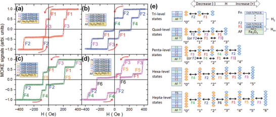
The construction of multilevel magnetic states using materials with perpendicular magnetic anisotropy (PMA) offers a novel approach to enhancing the storage density and read/write efficiency of nonvolatile magnetic memory devices. In this study, optically readable multilevel magnetic domain states are achieved by inducing asymmetric interlayer interactions and decoupling the magnetic reversal behavior of individual ferromagnetic (FM) layers in exchange-biased FM multilayers with PMA. Hepta-level magnetic domain states are formed in [Co/Pt]n FM multilayers grown on an antiferromagnetic Fe2O3 layer within a relatively low magnetic field range of ∼±400 Oe. Raising and lowering operations between states are demonstrated to be achievable, enabling the writing of new information without the need for initialization in multilevel magnetic memory applications. This design concept, leveraging multilevel magnetic domain states and facilitating noncontact optical reading of stored information, demonstrates the potential to enhance the storage density of nonvolatile magnetic memory devices as it eliminates the need for electrical circuits typically required in other resistive memory technologies.
Keywords: exchange‐biased ferromagnetic multilayers; magnetic states; memory devices; perpendicular magnetic anisotropy materials.
© 2025 The Author(s). Small published by Wiley‐VCH GmbH.
Conflict of interest statement
The authors declare no conflict of interest.
Figures


Similar articles
-
Effect of Composition and Thickness on the Perpendicular Magnetic Anisotropy of (Co/Pd) Multilayers.Sensors (Basel). 2017 Nov 28;17(12):2743. doi: 10.3390/s17122743. Sensors (Basel). 2017. PMID: 29182539 Free PMC article.
-
Ferromagnetic resonance measurements of (Co/Ni/Co/Pt) multilayers with perpendicular magnetic anisotropy.J Phys D Appl Phys. 2016;49(42):https://doi.org/10.1088/0022-3727/49/42/425002. J Phys D Appl Phys. 2016. PMID: 33100381 Free PMC article.
-
Oscillatory interlayer exchange coupling and its temperature dependence in [Pt/Co]3/NiO/[Co/Pt]3 multilayers with perpendicular anisotropy.Phys Rev Lett. 2003 Jul 18;91(3):037207. doi: 10.1103/PhysRevLett.91.037207. Epub 2003 Jul 17. Phys Rev Lett. 2003. PMID: 12906450
-
Domain size and structure in exchange coupled [Co/Pt]/NiO/[Co/Pt] multilayers.J Phys Condens Matter. 2011 Sep 21;23(37):376002. doi: 10.1088/0953-8984/23/37/376002. Epub 2011 Aug 31. J Phys Condens Matter. 2011. PMID: 21878718
-
Readable High-Speed Racetrack Memory Based on an Antiferromagnetically Coupled Soft/Hard Magnetic Bilayer.Nanomaterials (Basel). 2019 Oct 30;9(11):1538. doi: 10.3390/nano9111538. Nanomaterials (Basel). 2019. PMID: 31671575 Free PMC article.
References
-
- Iwasaki S.‐I., J. Magn. Magn. Mater. 2012, 324, 244.
-
- Osaka T., Asahi T., Kawaji J., Yokoshima T., E. Acta 2005, 50, 4576.
-
- Bhatti S., Sbiaa R., Hirohata A., Ohno H., Fukami S., Piramanayagam S. N., Mater. Today 2017, 20, 530.
-
- Chen A., Solid State Electro. 2016, 125, 25.
-
- Zhang G., Hwang W. S., Lee S.‐H., Cho B.‐J., Yoo W. J., IEEE Trans. Electron Devices 2008, 55, 2361.
Grants and funding
LinkOut - more resources
Full Text Sources
