Review
. 2025 Mar;37(10):e2418280.
doi: 10.1002/adma.202418280. Epub 2025 Jan 31.

Advances and Challenges in SnTe-Based Thermoelectrics

Affiliations
Review

Advances and Challenges in SnTe-Based Thermoelectrics

Lijun Wang et al. Adv Mater. 2025 Mar.

Abstract

SnTe-based thermoelectric materials have attracted significant attention for their exceptional performance in mid-to-high temperature ranges, positioning them as promising candidates for thermoelectric power generation. However, their efficiency is constrained by challenges related to electronic structure, defect chemistry, and phonon behavior. This review comprehensively summarizes advancements in SnTe thermoelectric materials and devices over the past five years, focusing on strategies to address these limitations. Key approaches include defect regulation, carrier transport optimization, and phonon engineering to enhance electrical conductivity, reduce thermal conductivity, and improve overall thermoelectric conversion efficiency. The review highlights breakthroughs in fabrication methods, doping and alloying, composite designs, and the development of novel nanostructures, with particular emphasis on 2D SnTe materials such as monolayers, bilayers, and thin films, which offer new opportunities for performance enhancement. Additionally, it provides an overview of SnTe-based thermoelectric devices, covering fabrication techniques, performance optimization, stability, and flexible device development. Despite significant progress, challenges remain in developing n-type SnTe materials, optimizing interfaces, ensuring long-term stability, and maximizing conversion efficiency. This review fills gaps in the existing literature and offers valuable insights and guidance for future research aimed at improving thermoelectric properties, advancing device integration, and driving the commercial viability of SnTe-based materials for practical applications.

Keywords: SnTe; device; material; structure; thermoelectric.


Conflict of interest statement

The authors declare no conflict of interest.

Figures

Figure 1
Figure 1
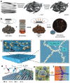
Exploring the characteristics and thermoelectric performance of SnTe‐based materials. a) Structural analysis of SnTe, showing Sn and Te atoms represented by large and small spheres, respectively. Copyright 2021, American Chemical Society. b) Phase diagram of the Sn‐Te system. c) Timeline of figure‐of‐merit (ZT) values for SnTe‐based materials over the past five years.[ 39 , 40 , 41 , 42 , 43 , 44 , 45 , 46 , 47 , 48 , 49 , 50 , 51 , 52 , 53 , 54 , 55 , 56 , 57 , 58 , 59 , 60 , 61 , 62 , 63 , 64 , 65 , 66 , 67 , 68 , 69 , 70 , 71 , 72 , 73 , 74 , 75 , 76 , 77 , 78 , 79 , 80 , 81 , 82 , 83 , 84 , 85 , 86 , 87 , 88 , 89 , 90 , 91 , 92 , 93 , 94 , 95 , 96 , 97 , 98 , 99 , 100 , 101 , 102 , 103 , 104 , 105 , 106 , 107 , 108 , 109 , 110 , 111 , 112 , 113 , 114 , 115 , 116 , 117 , 118 , 119 , 120 , 121 , 122 , 123 , 124 , 125 , 126 , 127 , 128 , 129 , 130 , 131 , 132 , 133 , 134 , 135 , 136 , 137 , 138 , 139 , 140 , 141 , 142 , 143 , 144 , 145 , 146 , 147 , 148 , 149 , 150 , 151 , 152 , 153 , 154 , 155 , 156 , 157 , 158 , 159 , 160 , 161 , 162 , 163 , 164 , 165 , 166 , 167 , 168 , 169 , 170 , 171 , 172 , 173 , 174 , 175 , 176 , 177 , 178 , 179 , 180 , 181 , 182 ] d) Temperature‐dependent ZT of typical bulk SnTe materials over the last five years.[ 39 , 48 , 62 , 64 , 111 , 123 , 124 , 141 , 163 , 165 ] e) Temperature difference (ΔT) dependence of thermoelectric conversion efficiency (η) in SnTe‐based thermoelectric devices.[ 40 , 84 , 96 , 107 , 120 , 160 , 183 ]
Figure 2
Figure 2
Band structures and interatomic interactions in pristine SnTe without spin‐orbit coupling. The orbital‐projected band structures of the pristine SnTe, excluding spin−orbit coupling (SOC), show the contributions from a) Sn‐s, b) Sn‐p, c) Te‐s, and d) Te‐p orbitals, represented by red, blue, green, and black dashed lines, respectively. VBM and VB2 denote the maximum valence band at the L point and the secondary maximum along the Σ‐line, respectively. e) Projected density of states (DOS) of SnTe without band inversion (no SOC). f) Diagram illustrating the interatomic interactions between Sn and Te atoms in the absence of band inversion. Reproduced with permission.[ 197 ] Copyright 2021, American Chemical Society.
Figure 3
Figure 3
Defect formation energies and charge density in SnTe‐based materials. a,b) Calculated defect formation energies of SnTe as a function of the fermi level under Sn‐rich and Sn‐poor conditions. Reproduced with permission.[ 203 ] Copyright 2021, Royal Society of Chemistry. c,d) Charge density maps and e,f) electron density difference maps of Mn‐ and Mg‐doped SnTe. Reproduced with permission.[ 204 ] Copyright 2023, Elsevier.
Figure 4
Figure 4
Contribution of phonon modes on lattice thermal conductivity. a) Computed phonon dispersion relations for SnTe across multiple high‐symmetry directions, along with the corresponding partial DOS (PDOS). b) Calculated anharmonic Grüneisen parameter (γ) across various high‐symmetry directions. c) Lattice thermal conductivity (κ l) as a function of phonon mean free path (MFP) at 300 and 500 K. d) κ l for different polarizations as a function of temperature. e) Contributions of various phonon modes to the overall thermal conductivity (κ). Reproduced with permission.[ 207 ] Copyright 2021, Elsevier.
Figure 5
Figure 5
Fabrication of SnTe‐based thermoelectric materials. a) SnTe single‐phase alloy produced by mechanical alloying and spark plasma sintering (SPS). Reproduced with permission.[ 214 ] Copyright 2023, Elsevier. b) Single‐phase SnTe‐based thermoelectric materials prepared by self‐propagating high‐temperature synthesis under high‐gravity field combined with SPS (SHS‐HG‐SPS) and c) different stages of the reaction. Reproduced with permission.[ 95 ] Copyright 2023, Royal Society of Chemistry. d) Post‐processing SnTe based bulk materials by constrained hot compressing. Optical images of SnTe‐based samples at different compression ratios (15%, 35%, and 55%) after constrained hot compressing: e) with aluminum sleeve, f) without aluminum sleeve. Reproduced with permission.[ 78 ] Copyright 2022, Elsevier.
Figure 6
Figure 6
Preparation and processing techniques for SnTe materials. a) Schematic diagram of the melt spinning process for preparing SnTe and digital photographs of typical SnTe melt spun strips. Reproduced with permission.[ 68 ] Copyright 2021, Elsevier. b) SnTe samples before saturation annealing and after saturation annealing. Reproduced with permission.[ 41 ] Copyright 2020, Royal Society of Chemistry. c) Fabrication of all‐length‐scale SnTe pellets by SPS extrusion process. Reproduced with permission.[ 157 ] Copyright 2020, Elsevier.
Figure 7
Figure 7
Band structure of SnTe with varying doping. a) Volume and formation energy of SnTe with varying VSn or SnTe Concentration. Here VSn denotes the Sn vacancy, and SnTe is the anti‐site defect (Sn substitute Te sites). b) Evolution of valence band in SnTe‐doped case. c) Direct bandgap at L (ΔL), and energy differences (ΔL−Σ) as functions of SnTe concentration (x). Band structure of d) pristine SnTe, e) SnTe‐doped, and f) InSn‐doped SnTe.[ 200 ] Here InSn is the anti‐site defect (In substitute Sn sites). Reproduced with permission.[ 200 ] Copyright 2020, Wiley. Schematic band structure of g) un‐doped SnTe at room temperature, h) impurity‐doped SnTe at low temperature, and i) impurity‐doped SnTe at high temperature. Reproduced with permission.[ 50 ] Copyright 2020, Elsevier.
Figure 8
Figure 8
Effects of electron doping on the properties of SnTe. a) Seebeck coefficient (S) and b) carrier mobility (µ) of pristine and electron‐doped (Ga, In, Bi, and Sb) SnTe as a function of carrier concentration (n) from the experiments (symbols) and the two‐band (TB) model calculations (lines). Reproduced with permission.[ 223 ] Copyright 2023, Wiley. c) The Fermi levels (dashed lines) of pristine SnTe and Sn0.97M0.03Te (M = Ga, In, Bi, and Sb) estimated by the TB model at 300 K.[ 223 ] Copyright 2023, Wiley. 3D response surfaces and contour plots of ZT for d) Zr‐doped SnTe and e) Ti‐doped of SnTe. Reproduced with permission.[ 60 ] Copyright 2024, Elsevier.
Figure 9
Figure 9
Phonon‐scattering mechanisms in Cu‐doped SnTe samples. a) Schematic representation of phonon‐scattering media from micro‐scale to atomic‐scale, with GB, TJ, and VdW indicating grain boundary, triple junction, and Van der Waals interactions. b) Calculated κ l as a function of temperature (T) based on the Debye–Callaway model, accounting for boundary scattering (B), Umklapp process phonon–phonon scattering (U), and point defect scattering (PD). c) Calculated κ l across typical thermoelectric operating temperatures for SnTe‐based compounds, alongside experimental κ l data for SnTe and (SnTe)0.94(Cu2Te)0.06. Reproduced with permission.[ 224 ] Copyright 2022, Wiley.
Figure 10
Figure 10
Band Structure, phonon scattering and mechanical properties in alloyed SnTe systems. a) Schematic of band structure engineering through alloying. b) Illustration of phonon scattering mechanisms from crystal imperfections in SnTe. Reproduced with permission.[ 91 ] Copyright 2021, Wiley. c) Contribution of different strengthening mechanisms to yield strength of the Sn0.93Mn0.10Te sample and comparison of the κ l between Sn1.03Te and Sn0.93Mn0.10Te sample, the inset shows the schematic diagram of the strengthening mechanisms in the Sn0.93Mn0.10Te sample, d) comparison of the room‐temperature compressive properties with some state‐of‐the‐art thermoelectric materials. e) Compressive stress‐strain curves for MnTe, with an inset optical image of MnTe samples before and after compressive testing. f–i) SEM images of Sn0.83Mn0.20 samples illustrating crack propagation. j) Diagrams depicting crack propagation. Reproduced with permission.[ 93 ] Copyright 2024, Wiley.
Figure 11
Figure 11
Band structure of SnTe with co‐doping. Unfolded band structures of a) Sn0.984Te, b) Sn0.968Ge0.016Te, c) Sn0.952Ge0.016Sb0.016Te, and d) Sn0.952Ge0.016As0.016Te. Reproduced with permission.[ 197 ] Copyright 2021, American Chemical Society.
Figure 12
Figure 12
Effects of alloying on the structure and electronic properties of SnTe. a) Simplified molecular orbital (MO) diagram for a SnTe6 octahedron. b) Modified MO diagram reflecting lattice contraction induced by NaSbTe2. c) Calculated PDOS for pure SnTe. d) Crystal orbital Hamiltonian plot (COHP) for SnTe, indicating bonding (positive values) and antibonding (negative values) character. Reproduced with permission.[ 100 ] Copyright 2020, American Chemical Society.
Figure 13
Figure 13
Effects of alloying on band structure and phonon transport properties of SnTe. a) Band structures of Sn27Te27 and Sn23Mn2CdGeTe27 with inclusion of spin–orbit coupling (SOC). The three‐valence band‐convergence related bands at L, Σ and Λ are labelled as 1, 2, and 3, respectively. Density functional theory (DFT) phonon dispersion of b) Sn8Te8 and c) Sn6MnCdTe8. Reproduced with permission.[ 39 ] Copyright 2024, Royal Society of Chemistry. d) Predicted structure diagrams of Sn–Sb–Te. Aberration‐corrected scanning transmission electron microscopy (STEM) high‐angle annular dark field (HAADF) image of Sb2Te3(SnTe)8 sample showing e) a 1D VSn line and f) a 2D VSn gap. g) STEM‐HAADF image of Sb2Te3(Sn0.996Re0.004Te)8 sample featuring an extended gap‐like structure. Reproduced with permission.[ 125 ] Copyright 2020, Royal Society of Chemistry.
Figure 14
Figure 14
Characterization of Sn0.87Mn0.08Sb0.08Te–5% AgSbTe2 microstructures. a) Atomic‐resolution HAADF‐STEM image and energy dispersive X‐ray spectrometry (EDS): mappings of the SnTe matrix (inset fast Fourier transform (FFT) image). b) 3D reconstruction of elemental distribution. c) Nearest‐neighbor atomic distribution histograms for five elements. d) Composition profile from a 100 nm cuboid region along the vertical direction. e) Low‐magnification HAADF‐STEM images of precipitates. f) HAADF‐STEM image of a Mn‐rich nanoprecipitate. g) High‐magnification HAADF‐STEM image of the Mn‐rich precipitate‐SnTe matrix interface (bright contrast). h) Annular bright‐field (ABF)‐STEM images depicting dislocations (darker lines). i) Atomic‐resolution HAADF‐STEM image of a dislocation line's disappearing area (inset FFT image). j) Strain mapping corresponding to the HRTEM image by geometrical phase analysis (strain range indicated on the color bar: −10–10%). Reproduced with permission.[ 141 ] Copyright 2022, Wiley.
Figure 15
Figure 15
Synthesis and characterization of SnTe Nanocomposites. a) Schematic representation of the MXene/SnTe nanocomposite synthesis route. Reproduced with permission.[ 168 ] Copyright 2021, Elsevier. b) Process for creating SnTe‐Bi2S3 nanocomposites. Reproduced with permission.[ 171 ] Copyright 2022, Wiley. c) Schematic diagram showing Cu‐rich grain boundary features resulting from chemical plating Cu. Reproduced with permission.[ 176 ] Copyright 2023, Elsevier. d) Diagram of the cation exchange reaction on SnTe powder surface. e) Schematic of the CuInTe2/SnTe core‐shell structure post‐exchange. f) Schematic of electrons and phonons transport characteristics in the coated grain nanocomposite. Reproduced with permission.[ 165 ] Copyright 2021, Royal Society of Chemistry.
Figure 16
Figure 16
Analyzing microstructure and composition to understand inhibited Ostwald ripening. Schematic representation depicting a) the standard mechanism of Ostwald ripening and b) the impact of interfacial complexions, resulting from Gibbs adsorption of Ag at interfaces, on slowing down Ostwald ripening. Reproduced with permission.[ 166 ] Copyright 2021, Royal Society of Chemistry.
Figure 17
Figure 17
Characterization of SnTe monolayers. a) Electronic band structures and partial density of states (PDOS) of SnTe monolayer calculated using Perdew‐Burke‐Ernzerhof (PBE) and hybrid density functional (HSE06). b) Spatial charge densities for the valence band maximum (VBM) and conduction band minimum (CBM) of the SnTe monolayer. c) Phonon dispersion relations and phonon DOS (PhDOS) for the SnTe monolayer. d) Vibrational modes of acoustic (LA, TA, ZA) and optical (LO, TO, ZO) phonon branches at the Γ point. e,f) ZT values of the SnTe monolayer along the zigzag‐ and armchair‐ directions as a function of carrier concentration at various temperatures. Here n h and n e represent the hole carrier concentration in p‐type materials and electron carrier concentration in n‐type materials. Reproduced with permission.[ 252 ] Copyright 2023, Elsevier.
Figure 18
Figure 18
Structural properties of precipitate in SnTe matrix. a) A unit cell of rhombohedral h‐SnTe and its projections along the crystallographic directions of b) [112¯0], c) [8412¯1], and d) [44¯01¯]. Reproduced with permission.[ 256 ] Copyright 2024, Royal Society of Chemistry. e) Structure model showing the overlap of the h‐SnTe with the β‐SnTe matrix along the [11¯0] β‐SnTe zone axis. f) ABF‐STEM images of the β‐SnTe sample along the [11¯0] β‐SnTe zone axis, with the region of interest (ROI) indicated by red arrows and the vdWs gaps shown by purple arrows. The FFT patterns of β‐SnTe and h‐SnTe are inserted, highlighting extra spots in h‐SnTe with a red arrow. g) HAADF‐STEM image of the β‐SnTe sample containing the ROI under electron beam irradiation (100s). h–j) Atomic‐resolution HAADF‐STEM images illustrating the formation of the h‐SnTe precipitate in the β‐SnTe matrix along the [11¯0] zone axis, captured at 20, 40, and 85 s under continuous electron‐beam irradiation, with structural models of β‐ and h‐SnTe superposed and vdWs gaps formation in h‐SnTe marked by oblique arrows. Reproduced with permission.[ 256 ] Copyright 2024, Royal Society of Chemistry.
Figure 19
Figure 19
Fabrication and testing of a SnTe‐based thermoelectric device (TED). a) Schematic representation of the fabrication process for the single‐leg thermoelectric device. Reproduced with permission.[ 97 ] Copyright 2024, American Chemical Society. b) Optimal images of the fabricated (Sn0.96Sb0.04Te)0.7(Ge0.5Mn0.5Te)0.3/Bi2Te2.7Se0.3 + 0.01 wt% BiCl3 thermoelectric module, along with a schematic diagram of the custom thermoelectric testing system. Reproduced with permission.[ 107 ] Copyright 2022, Elsevier.
Figure 20
Figure 20
Characterization and performance of the SnTe‐based thermoelectric module. a) Connection of the Cu electrode to the p‐type Sn0.88Mn0.12Li0.01Te leg using AgCu‐based solder. b) Scanning electron microscopy (SEM) image of the Cu electrode and p‐type leg joint by transient liquid phase (TLP) bonding. c) Back‐scattered electron (BSE) images of the TLP bonding joint after treatment at 873 K for 24 h. d) Simulated maximum η and e) output power density (P d) as functions of the leg area ratio (A p/A n) and leg height (H) for the module. f) Optical images showing the module before and after testing. Reproduced with permission.[ 84 ] Copyright 2022, Elsevier.
Figure 21
Figure 21
Characterization and performance of the SnTe‐based thermoelectric module. a) Optical images of the 17‐couple SnTe‐based thermoelectric module. b) Measured η as a function of ΔT, along with comparative data from other thermoelectric modules. Reproduced with permission.[ 40 ] Copyright 2022, Wiley. c) Photograph of the assembled all‐SnTe‐based seven‐pair TED. d) Mini‐PEM testing for power generation performance. e) Measured η as a function of current (I) at various hot‐side temperatures (T h), with the cold‐side temperature (T c) held at ≈298 K. f) Maximum η at different ΔTs. Reproduced with permission.[ 120 ] Copyright 2024, American Chemical Society.
Figure 22
Figure 22
Characterization of flexible SnTe–based thin film thermoelectric device (TED). a) Image of the large‐area flexible TED featuring 32 thermoelectric pairs. b) Real‐time demonstration of the TED functioning as a wearable power source by illuminating an LED with body heat. c) Variation in internal resistance with the number of heating cycles. d) Internal resistance changes of the TED with the number of bending cycles (bending radius = 3 cm) at ambient temperature. Reproduced with permission.[ 267 ] Copyright 2020, Elsevier.
Figure 23
Figure 23
Evolution of SnTe intermetallic compound layers at the Bi‐Sb‐Te/Sn interface. a) Schematic representation of the development of intermetallic compound (IMC) layers and phase compositions at the Bi‐Sb‐Te/Sn interface during aging. b) Schematic illustration of the atomic arrangement and growth direction of phases within the IMC layers at the β‐Sn/Sn‐Sb/Sn‐Bi‐Sb‐Te/Bi‐Sb‐Te multi‐interfaces. Reproduced with permission.[ 272 ] Copyright 2023, Elsevier.
Figure 24
Figure 24
Challenges and outlooks for SnTe‐based thermoelectrics.

References

    1. Geffroy C., Lilley D., Parez P. S., Prasher R., Joule 2021, 5, 3080.
    1. Qin B., Wang D., Liu X., Qin Y., Dong J.‐F., Luo J., Li J.‐W., Liu W., Tan G., Tang X., Li J.‐F., He J., Zhao L.‐D., Science 2021, 373, 556. - PubMed
    1. Bell L. E., Science 2008, 321, 1457. - PubMed
    1. Qin B., Kanatzidis M. G., Zhao L.‐D., Science 2024, 386, adp2444. - PubMed
    1. Shi X.‐L., Zou J., Chen Z.‐G., Chem. Rev. 2020, 120, 7399. - PubMed

LinkOut - more resources