. 2025 Mar 5;25(9):3375-3382.
doi: 10.1021/acs.nanolett.4c04252. Epub 2025 Feb 5.

Giant Light Emission Enhancement in Strain-Engineered InSe/MS2 (M = Mo or W) van der Waals Heterostructures

Affiliations

Giant Light Emission Enhancement in Strain-Engineered InSe/MS2 (M = Mo or W) van der Waals Heterostructures

Elena Blundo et al. Nano Lett. .

Abstract

Two-dimensional (2D) heterostructures (HSs) offer unlimited possibilities for playing with layer number, order, and twist angle. The realization of high-performance optoelectronic devices, however, requires the achievement of specific band alignments, k-space matching between conduction and valence band extrema, and efficient charge transfer between the constituent layers. Fine-tuning mechanisms to design ideal HSs are lacking. Here, we show that layer-selective strain engineering can be exploited as an extra degree of freedom to tailor the band alignment and optical properties of 2D HSs. To that end, strain is selectively applied to MS2 (M = Mo or W) monolayers in InSe/MS2 HSs, triggering a giant photoluminescence enhancement of the highly tunable but weakly emitting InSe of up to >2 orders of magnitude. Resonant excitation measurements, supported by first-principles calculations, provide evidence of a strain-activated charge transfer from the MS2 monolayers toward InSe. The huge emission enhancement of InSe widens its range of applications for optoelectronics.

Keywords: 2D materials; InSe; heterostructures; strain; transition metal dichalcogenides.


Conflict of interest statement

The authors declare no competing financial interest.

Figures

Figure 1
Figure 1
Heterostructured InSe/TMD bubbles. (a) Sketch of the band structure of few-layer-thick InSe and one-layer-thick TMDs. The effect of strain on the VB of TMDs is highlighted. For high strains, the valley at Γ goes above that at K and direct (green) and indirect (cyan) excitons hybridize. (b) Sketch of the system studied in this work, consisting of a heterostructured bubble. A few-layer-thick InSe flake is deposited atop a strained TMD ML in the shape of a bubble; hBN is used to cap the system. (c) Optical image of a flake with heterostructured bubbles. (d) AFM image of the bubble within the white rectangle in panel c.
Figure 2
Figure 2
(a) Giant InSe emission enhancement in selectively strained InSe/MS2 heterostructures. (a) μ-PL spectra at 300 and 5 K of two HS bubbles (one with MoS2 as the TMD, left, and one with WS2, right) and of the region right outside the bubble, as indicated in the sketch in panel (b). (c) Summary of the ratios between the PL intensity in the HS bubbles and outside, measured in several MoS2- and WS2-based structures at 5 or at 300 K.
Figure 3
Figure 3
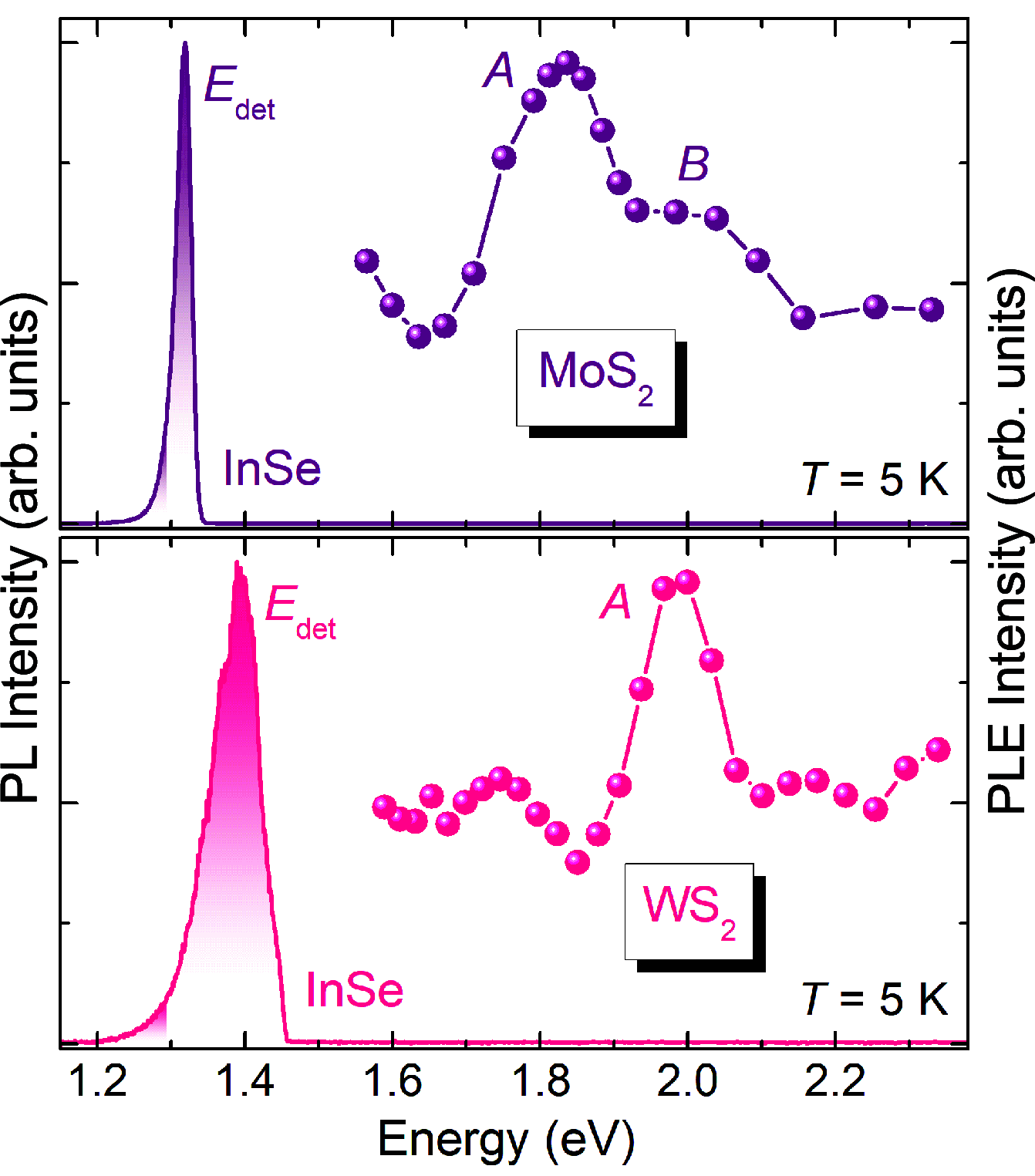
Energy-resonant photoexcited carrier transfer. PLE spectra of (a) a HS bubble based on MoS2 and (b) a HS bubble based on WS2. The corresponding PL band whose intensity was detected during the PLE measurements is displayed. Exciton resonances attributable to the A and B excitons of the TMD are highlighted.
Figure 4
Figure 4
Heterostructured bubble band alignment. DFT-calculated band structures of (a) a MoS2 ML with S vacancies at 0% strain, (b) a 6L InSe slab, and (c) a MoS2 ML at 2% biaxial strain. The shaded regions mark the VB and CB of 6L InSe in all panels. The inset of panel c shows a close-up of the top VB of strained MoS2 at the Γ and K points.

References

    1. Blundo E.; Yildirim T.; Pettinari G.; Polimeni A. Experimental adhesion energy in van der Waals crystals and heterostructures from atomically thin bubbles. Phys. Rev. Lett. 2021, 127, 046101.10.1103/PhysRevLett.127.046101. - DOI - PubMed
    1. Geim A. K.; Grigorieva I. V. Van der Waals heterostructures. Nature 2013, 499, 419.10.1038/nature12385. - DOI - PubMed
    1. Cao Y.; Fatemi V.; Fang S.; Watanabe K.; Taniguchi T.; Kaxiras E.; Jarillo-Herrero P. Unconventional superconductivity in magic-angle graphene superlattices. Nature 2018, 556, 43.10.1038/nature26160. - DOI - PubMed
    1. Britnell L.; Gorbachev R. V.; Jalil R.; Belle B. D.; Schedin F.; Mishchenko A.; Georgiou T.; Katsnelson M. I.; Eaves L.; Morozov S. V.; Peres N. M.; Leist J.; Geim A. K.; Novoselov K. S.; Ponomarenko L. A. Field-effect tunneling transistor based on vertical graphene heterostructures. Science 2012, 335, 947.10.1126/science.1218461. - DOI - PubMed
    1. Georgiou T.; Jalil R.; Belle B. D.; Britnell L.; Gorbachev R. V.; Morozov S. V.; Kim Y.-J.; Gholinia A.; Haigh S. J.; Makarovsky O.; Eaves L.; Ponomarenko L. A.; Geim A. K.; Novoselov K. S.; Mishchenko A. Vertical field-effect transistor based on graphene–WS2 heterostructures for flexible and transparent electronics. Nat. Nanotechnol. 2013, 8, 100.10.1038/nnano.2012.224. - DOI - PubMed

LinkOut - more resources