Review
. 2025 Mar;12(9):e2413679.
doi: 10.1002/advs.202413679. Epub 2025 Feb 8.

Bottom-Up Metasurfaces for Biotechnological Applications

Affiliations
Review

Bottom-Up Metasurfaces for Biotechnological Applications

Francesca Petronella et al. Adv Sci (Weinh). 2025 Mar.

Abstract

Metasurfaces are the 2D counterparts of metamaterials, and their development is accelerating rapidly in the past years. This progress enables the creation of devices capable of uniquely manipulating light, with applications ranging from optical communications to remote biosensing. Metasurfaces are engineered by rational assembly of subwavelength elements, defined as meta-atoms, giving rise to unique physical properties arising from the collective behavior of meta-atoms. These meta-atoms are typically organized using effective, reproducible, and precise nanofabrication methods that require a lot of effort to achieve scalable and cost-effective metasurfaces. In contrast, bottom-up methods based on colloidal nanoparticles (NPs) have developed in the last decade as a fascinating alternative for accelerating the technological spread of metasurfaces. The present review takes stock of recent advances in the fabrication and applications of hybrid metasurfaces prepared by bottom-up methods, resulting in disordered metasurfaces. In particular, metasurfaces prepared with plasmonic NPs are emphasized for their multifold applications, which are discussed from a biotechnology perspective. However, some examples of organized metasurfaces prepared by merging bottom-up and top-down approaches are also described. Finally, leveraging the historical disordered metasurface evolution, the review draws new perspectives for random metasurface design and applications.

Keywords: biosensing; biotechnologies; metasurfaces; optics; pathogens; photo‐thermal; plasmonics.


Conflict of interest statement

The authors declare no conflict of interest.

Figures
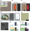
Figure 1
Figure 1
a) Scanning electron microscopy (SEM) micrograph of a flawless absorber surface of AgNCs covering an Au film. The inset shows the cross‐section of a single subwavelength resonator. Images of the Akselrod metasurface (b) and an Au film (c) illuminated by a defocused 645 nm laser. The metasurface shows no reflection (b), while the Au film reflects the laser (c). d) Image of the Akselrod metasurface on a glass half‐sphere, deposited through conformal deposition. The SEM image of the sample's side slope and the near‐normal incidence reflectance spectrum are shown in the insets. Reproduced with permission.[ 16 ] 2015, WILEY‐VCH Verlag GmbH and Co. KGaA, Weinheim. e) Optical microscopy image of the metasurface reported by Petronella et al., accompanied by the corresponding SEM micrograph (f).[ 17 ] Reproduced under terms of the CC‐BY license.[ 17 ] 2023, Petronella et al., published by American Chemical Society. g–j) Fabrication process used by Kim et al. for developing a tunable plasmonic nanofilter.[ 20 ] The process involves three steps: electrodeposition of PANI on an ITO substrate, physical deposition of thin Au to form AuNPs on PANI, and final electrodeposition of PANI to encapsulate the AuNPs. Reproduced under terms of the CC‐BY license.[ 20 ] 2024, Gyurin Kim et al., published by Springer Nature.
Figure 2
Figure 2
a) Assembly scheme for the large area metasurface investigated by Zheng et al. a,b) creating a 2D crystalline SLs.[ 21 ] PAE monomers are heated for several hours above the melting point‐temperature of their assembled aggregates (T M,agg) b) UV–vis melting curves, measured at λ = 550 nm, demonstrating temperature‐dependent intensity value. T C = 68 °C is the temperature at which there is an equilibrium between crystalline SLs and the melt. The crystallization is facilitated at T C. Reproduced with permission.[ 21 ] 2021, American Chemical Society. c) Illustration of several colloidal NPs shapes that self‐assemble on a transparent substrate, d) schematic of the procedure used by Stewart et al. for realizing the self‐assembly of colloidal NPs, with different morphology, on a transparent substrate. Reproduced with permission.[ 22 ] 2022, American Chemical Society. e) AuNRs trimers patterning composing the flexible chiral metasurfaces produced by H. T. Lin et al.[ 23 ] Reproduced with permission.[ 23 ] 2022, The Royal Society of Chemistry. f) Schematic representation of the preparation procedure proposed by Zhou et al.[ 24 ] to control the orientation and position of prismatic NPs utilizing shallow holes for locally anchoring prismatic NPs, as presented in the respective SEM image. Reproduced with permission.[ 24 ] 2020, Published under the PNAS license.
Figure 3
Figure 3
a) Schematic of the metasurface studied by Rozin et al.[ 18 ] b) Simulated reflectance spectra of Rozin's metasurface calculated for different interparticle distances. c) Fundamental resonance wavelength variation as a function of interparticle distance. d) Variation of the FWHM as a function of interparticle distance. e) Calculated magnetic and electric field intensities for a close‐packed metasurface (d = 4 nm) at the fundamental resonance wavelength (λ = 2.54 µm). f,g) Variation of the fundamental resonance wavelength as a function of nanocube size (f) and spacer height (g), obtained via 2D FDTD simulations. h) Fundamental resonance wavelength variation for metasurfaces with domains of meta‐atoms (AgNCs) of different sizes, along with corresponding SEM micrographs (scale bar: 500 nm). i–l) SEM micrographs (scale bar: 500 nm) of low‐density metasurfaces using NCs (i), spheroids (j), and octahedra (k) as meta‐atoms, demonstrating shape‐dependent optical properties (l). m–p) SEM micrographs (scale bar: 500 nm) of close‐packed metasurfaces using NCs (m), spheroids (n), and octahedra (o) as meta‐atoms, showing shape‐dependent optical properties (p). Reproduced under terms of the CC‐BY license.[ 18 ] 2015, Matthew J. Rozin et al., published by Springer Nature.
Figure 4
Figure 4
a) Simulated reflection spectra for three metasurfaces made up of the three NP morphologies displayed in Figure 2e. They demonstrate how the plasmonic cavity's geometry affects the wavelength of resonant absorption. b) Electric field enhancement of these geometries at the fundamental plasmon resonance. Reproduced with permission.[ 22 ] 2022, American Chemical Society. c) CD magnitude variation obtained by the controlled stretching of the substrate realized by H. T. Lin et al.[ 23 ] d) CD extinction stretching the substrate along the y and x‐axes. Reproduced with permission.[ 23 ] 2022, The Royal Society of Chemistry.
Figure 5
Figure 5
a) Theoretical and experimental study on the sensitivity of the metasurface to n changes, as shown by the image of the metasurface (b) and the metasurface cell during infiltration with NOA‐61 (c), which demonstrates a significant color change (d). e) Schematic illustration of the adopted customized spectroscopic‐photo‐thermal apparatus.[ 17 ] Reproduced under terms of the CC‐BY license.[ 17 ] 2023, Petronella et al., published by American Chemical Society.
Figure 6
Figure 6
a) AuNRs immobilized on a PEM‐coated glass substrate. The metasurface was functionalized with an antibody for E. coli detection. Reproduced with permission.[ 27 ] 2022, The Royal Society of Chemistry. b) AuNPs on APTES‐coated glass. Functionalization occurred with an aptamer to detect S. typhimurium. Reproduced with permission.[ 32 ] 2017, Springer Nature c) AuNPs and AgNPs on APTES coated PDMS substrate. Functionalization occurred with an aptamer to detect S. aureus. ROX and another layer of AuNPs and AgNPs were used as Raman reporters. Reproduced with permission.[ 33 ] 2023, Elsevier B.V. d) AuNPs and Au electrodes separated by L‐cysteine layer to detect Norovirus. Reproduced with permission.[ 36 ] 2024, The Royal Society of Chemistry. e) SEM image of the optical metasurface integrated into the multifunctional face mask. f) Photo of the optical metasurface biosensor integrated on the FFP2 face mask functionalized surface. g) Calibration curve of the E. coli qualitative and quantitative detection. Reproduced with permission.[ 37 ] 2024, Wiley‐VCH GmbH.
Figure 7
Figure 7
Optical metasurfaces for biomedical applications. a) Photo highlighting the peculiar diffraction of light of the 70 nm Au evaporated Blu‐Ray disc substrate (on the left) and SEM micrograph of the plasmonic nanocrystals (on the right). b) Reflectance spectra obtained at different concentrations of spiked cell culture showing the plasmonic band displacement. c) Calibration curve of the IL‐6 detection.[ 40 ] Reproduced under terms of the CC‐BY license.[ 40 ] 2021, The Authors, published by De Gruyter. d) Schematic representation of the procedure for the substrate to capture epithelial cell adhesion molecule protein. Reproduced with permission.[ 44 ] 2018, American Chemical Society. e) Schematic representation of the specific process of this detection strategy, detecting TYR activity. Reproduced with permission.[ 42 ] 2022, American Chemical Society.
Figure 8
Figure 8
Self‐assembled optical metasurfaces applied in the biomedical field. a) On the left is the IR thermal imaging schematic of the disordered bottom‐up metasurface under a laser source. On the right are photographs of the four metasurfaces fabricated with a dielectric spacer with 60, 280, 340, and 410 nm of thickness. b) Thermal images of the metasurfaces irradiated under 405, 473, 532, and 633 nm laser sources. Reproduced with permission.[ 55 ] 2023, American Chemical Society. c) Optical absorption spectroscopy of the hybrid heterostructure. d) Diffuse reflectance spectroscopy of the functionalized FFP2 face mask fibers. e) SEM micrograph of the functionalized FFP2 face mask fibers. (Inset) Transmission electron microscopy (TEM) micrograph of the heterostructures composed of AgNCs surrounded by AuNRs. f) Photo of the bare face mask on the left and of the reddish functionalized face mask on the right. g) High‐resolution thermal image and h) photo of the functionalized FFP2 face mask irradiated by the white light source. i) Colony counting of the bacterial cells after different irradiation time intervals. Reproduced with permission.[ 37 ] 2024, Wiley‐VCH GmbH.

References

    1. Katiyi A., Karabchevsky A., In Reference Module in Materials Science and Materials Engineering, Elsevier, Amsterdam, 2022.
    1. Qin F., Peng H.‐X., Prog. Mater. Sci. 2013, 58, 183.
    1. Govindaraman L. T., Arjunan A., Baroutaji A., Robinson J., Olabi A.‐G., In Encyclopedia of Smart Materials, Elsevier, Amsterdam, 2022, 2, pp. 522–534.
    1. Nemati A., Wang Q., Hong M. H., Teng J. H., Opto‐Electron. Adv. 2018, 1, 180009.
    1. Kuznetsov A. I., Brongersma M. L., Yao J., Chen M. K., Levy U., Tsai D. P., Zheludev N. I., Faraon A., Arbabi A., Yu N., Chanda D., Crozier K. B., Kildishev A. V., Wang H., Yang J. K. W., Valentine J. G., Genevet P., Fan J. A., Miller O. D., Majumdar A., Fröch J. E., Brady D., Heide F., Veeraraghavan A., Engheta N., Alù A., Polman A., Atwater H. A., Thureja P., Paniagua‐Dominguez R., et al., ACS Photonics 2024, 11, 816. - PMC - PubMed

LinkOut - more resources