. 2025 Feb 26;25(8):3059-3065.
doi: 10.1021/acs.nanolett.4c05016. Epub 2025 Feb 13.

Lithography-Free Water Stable Conductive Polymer Nanowires

Affiliations

Lithography-Free Water Stable Conductive Polymer Nanowires

Damien Hughes et al. Nano Lett. .

Abstract

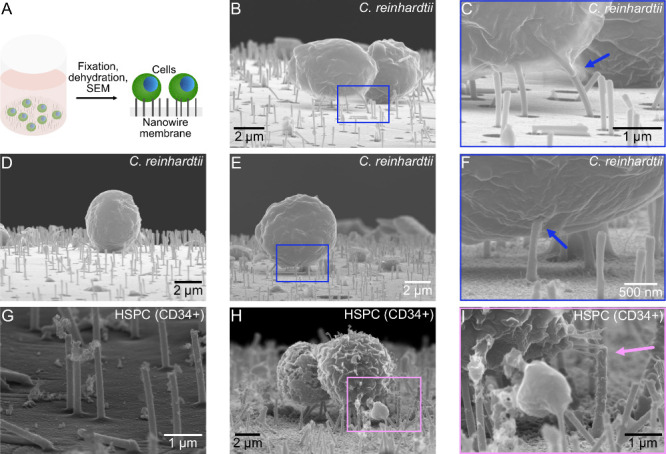
Free-standing nanowires can gain intracellular access without causing stress or apoptosis. Current approaches to generate nanowires focus on lithographic patterning and inorganic materials (Si, GaAs, Al2O3, etc.) while organic materials are less explored. Use of organic conductive polymers allows for the creation of soft mixed ion-electron conducting nanowires. Processing conductive polymers into nanowires is challenging due to the harsh chemicals and processing conditions used. Here, we demonstrate a lithography-free and scalable method to generate all-organic, water-stable nanowires composed of conductive polymers. A nanoporous membrane is filled with conductive polymer in solution, followed by a cross-linking step to make the polymer water stable. The surface of the membrane is anisotropically etched using a reactive ion etcher to reveal the polymer inside the pores, which extends from the membrane as nanowires. We interface the nanowires with model algal cells and human primary hematopoietic stem and progenitor cells.

Keywords: PEDOT-S; algae; bioelectronics; cellular interfacing; conductive polymer; nanowires.


Conflict of interest statement

The authors declare no competing financial interest.

Figures

Figure 1
Figure 1
NW processing. (A) Schematic side view describing the processing. A track-etched (TE) membrane is filled with CP solution and then allowed to dry. After drying, excess CP is removed. The TE membrane is then dry-etched using oxygen-based inductively coupled plasma reactive ion etching (ICP-RIE) to reveal the NWs. Please note that the schematic is not to scale. (B–E) 30° tilted view SEM images of NWs of various lengths. Length can be controlled by modifying the etch time. The etching times used were 1 min (B), 2 min (C), 3 min (D), and 4 min (E). (F–I) 30° tilted view SEM images of NWs made to have different thicknesses due to varying pore diameter. The pore diameters used were 160 nm (F), 200 nm (G), 250 nm (H), and 300 nm (I). (J, K) 30° tilted SEM images showing different pore densities: 5.5 × 107 cm–2 for panel J and 2 × 107 cm–2 for panel K. (L) Photograph of processed NWs on polyimide membrane. The photograph showcases both flexibility and transparency of the material. (M, N) Graphs illustrating the effects of pore size (M) and etch time (N) on NW length and diameter. The dots on the graph represent the mean (14–33 NWs measured per dot), while the error bars represent the standard deviation. The scale bars are 100 nm in B–I and 1 μm in J and K.
Figure 2
Figure 2
NW stability can be increased by incorporating trimers and electrofunctionalization or chemical strengthening. (A–J) NW stability after being submerged in PBS up to 10 days. (A) Timeline of PBS exposure to NWs. (B–E) 30° tilted SEM images of NW strengthened with trimers and 100 mM Fe3+. NWs were imaged before exposure to PBS (B, F), after 3 days of exposure (C, G), after 7 days of exposure (D, H), and after 10 days of exposure (E, I). Lower magnification images of NWs after exposure available in Figure S6. (J) Graph illustrating the NW diameter and NW length at various time points. Dots on the graph represent the mean, while error bars represent the standard deviation. (K–M) 30° tilted view SEM images of NWs electrofunctionalized with ETE-S. In K, the white arrow indicates the plasticizers inherent to the TE membrane, and the green arrows indicate the holes left from the plasticizers. The scale bars are 100 nm for panels B–E and M, 1 μm for panels F–I and L, and 10 μm for panel K.
Figure 3
Figure 3
Physical characterization of NWs was performed by conductive atomic force microscopy (cAFM). Panels A and E are diagrams illustrating cAFM configuration, panels B–D are measurements taken on NWs lying flat on a surface, while panels F–H are measurements on standing NWs still embedded in a TE membrane. Topography images, both in 2D (B, C, G) and 3D (F) representation, range from white at the highest point, brown at midpoint, to black at the lowest point. Current maps (D, H) express light green at the most conductive point, then range through blue, and purple at the midpoints, then to black at the least conductive point. (B) Topography image of NW height. The image shows a single NW lying on a patterned surface, part of the NW on the gold section, and the rest of the NW on the glass surface. The gold section is denoted by the dotted yellow line, while the rest of the image is the glass surface. (C, D) Topography image of height (C) and current map (D) on a section of the same NW as shown in B. (F) Three-dimensional representation of cAFM height measurements on NWs. (G, H) Two-dimensional topography (G) and current map (H) on standing NWs.
Figure 4
Figure 4
Interfacing living cells with CP NWs stabilized by 10 mM Fe3+. (A) Schematic depicting cells added to a culture vessel incorporating the NW membrane in the bottom. Following fixation and dehydration, the sample is imaged from the side to reveal the NWs interfacing with the cells. (B–F) SEM images showing algal cells, C. reinhardtii, on the NWs. Panels C, F, I are zoomed in from the marked regions in panels B, E, H. Blue arrows show NWs seemingly reaching inside the cells. (G–I) SEM images showing human primary hematopoietic stem cells (HSPCs, CD34+) interfacing NWs. Image G was obtained in a cell-free region. The pink arrow in I depicts cells reaching out to grab the spikes.

References

    1. Zhang Z.; Lamers N.; Sun C.; Hetherington C.; Scheblykin I. G.; Wallentin J. Free-Standing Metal Halide Perovskite Nanowire Arrays with Blue-Green Heterostructures. Nano Lett. 2022, 22 (7), 2941–2947. 10.1021/acs.nanolett.2c00137. - DOI - PMC - PubMed
    1. Behrman K.; Kymissis I. Micro light-emitting diodes. Nature Electronics 2022, 5 (9), 564–573. 10.1038/s41928-022-00828-5. - DOI
    1. Ram M. S.; Persson K.-M.; Irish A.; Jönsson A.; Timm R.; Wernersson L.-E. High-density logic-in-memory devices using vertical indium arsenide nanowires on silicon. Nature Electronics 2021, 4 (12), 914–920. 10.1038/s41928-021-00688-5. - DOI
    1. Li Z.; Song J.; Mantini G.; Lu M.-Y.; Fang H.; Falconi C.; Chen L.-J.; Wang Z. L. Quantifying the Traction Force of a Single Cell by Aligned Silicon Nanowire Array. Nano Lett. 2009, 9 (10), 3575–3580. 10.1021/nl901774m. - DOI - PubMed
    1. Cao Y.; Hjort M.; Chen H.; Birey F.; Leal-Ortiz S. A.; Han C. M.; Santiago J. G.; Paşca S. P.; Wu J. C.; Melosh N. A. Nondestructive nanostraw intracellular sampling for longitudinal cell monitoring. Proc. Natl. Acad. Sci. U. S. A. 2017, 114 (10), E1866–E1874. 10.1073/pnas.1615375114. - DOI - PMC - PubMed