

Recent advances in CMOS-compatible synthesis and integration of 2D materials
- PMID: 39954210
- PMCID: PMC11829894
- DOI: 10.1186/s40580-025-00478-1
Recent advances in CMOS-compatible synthesis and integration of 2D materials
Abstract
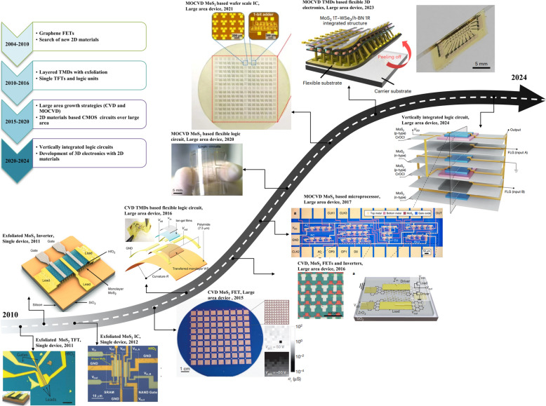
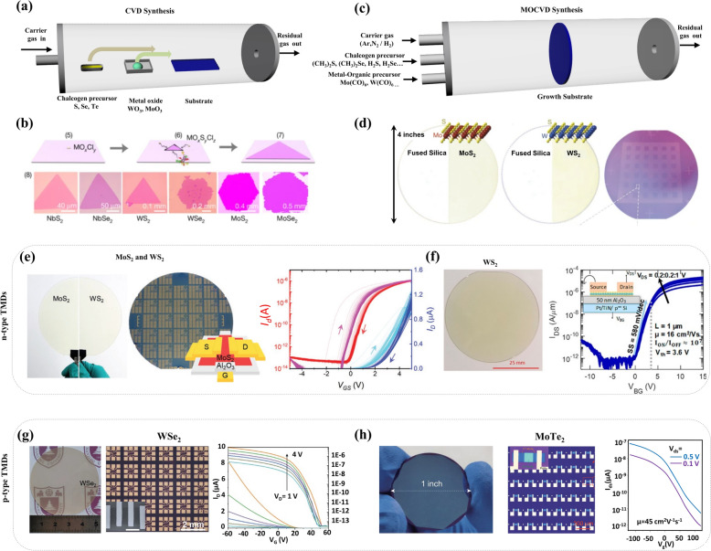
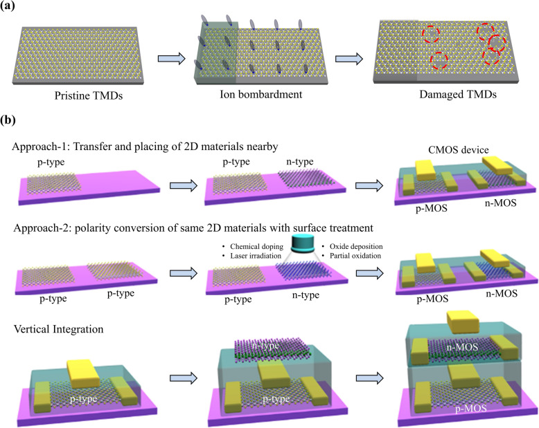
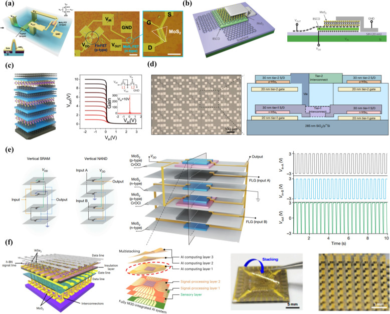
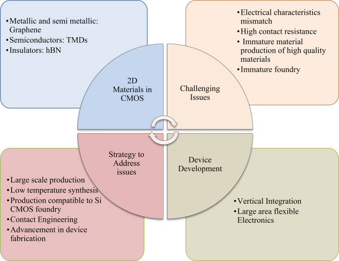
The upcoming generation of functional electronics in the era of artificial intelligence, and IoT requires extensive data storage and processing, necessitating further device miniaturization. Conventional Si CMOS technology is struggling to enhance integration density beyond a certain limit to uphold Moore's law, primarily due to performance degradation at smaller dimensions caused by various physical effects, including surface scattering, quantum tunneling, and other short-channel effects. The two-dimensional materials have emerged as highly promising alternatives, which exhibit excellent electrical and mechanical properties at atomically thin thicknesses and show exceptional potential for future CMOS technology. This review article presents the chronological progress made in the development of two-dimensional materials-based CMOS devices with comprehensively discussing the advancements made in material production, device development, associated challenges, and the strategies to address these issues. The future prospects for the use of two-dimensional materials in functional CMOS circuitry are outlooked, highlighting key opportunities and challenges toward industrial adaptation.
Keywords: 2D materials; CMOS devices; Flexible electronics; M3D integration; TMDs.
© 2025. The Author(s).
Conflict of interest statement
Declarations. Competing interests: The authors declare that they have no competing interests.
Figures


References
-
- S. Reggiani, E. Gnani, A. Gnudi, M. Rudan, G. Baccarani, Low-field electron mobility model for ultrathin-body SOI and double-gate MOSFETs with extremely small silicon thicknesses. IEEE Trans. Electron Dev. 54, 2204 (2007). 10.1109/TED.2007.902899
-
- K. Uchida, H. Watanabe, A. Kinoshita, J. Koga, T. Numata, and S. Takagi, in Digest. International Electron Devices Meeting (IEEE, 2002), pp. 47. 10.1109/IEDM.2002.1175776
-
- K.S. Novoselov, A.K. Geim, S.V. Morozov, D. Jiang, Y. Zhang, S.V. Dubonos, I.V. Grigorieva, A.A. Firsov, Electric field effect in atomically thin carbon films. Science 306, 666 (2004). 10.1126/science.1102896 - PubMed
-
- B. Radisavljevic, A. Radenovic, J. Brivio, V. Giacometti, A. Kis, Single-layer MoS2 transistors. Nat. Nanotechnol. 6, 147 (2011). 10.1038/nnano.2010.279 - PubMed
-
- H. Shin et al., Nonconventional strain engineering for uniform biaxial tensile strain in MoS2 thin film transistors. ACS Nano 18, 4414 (2024). 10.1021/acsnano.3c10495 - PubMed
Publication types
LinkOut - more resources
Full Text Sources