. 2025 Jun;21(24):e2410892.
doi: 10.1002/smll.202410892. Epub 2025 Mar 3.

Infrared-Triggered Retinomorphic Artificial Synapse Electronic Device Containing Multi-Dimensional van der Waals Heterojunctions

Affiliations

Infrared-Triggered Retinomorphic Artificial Synapse Electronic Device Containing Multi-Dimensional van der Waals Heterojunctions

Soobin Shim et al. Small. 2025 Jun.

Abstract

Biological systems excel in image recognition with low power and fast responses. Inspired by the human eye, researchers have developed solid-state artificial visual systems. In this study, a retinomorphic artificial synapse device based on a tungsten diselenide (WSe2)/indium arsenide quantum dot (InAs QD) heterostructure is developed. This device exhibits enhanced short-wavelength infrared (SWIR) responsivity at 1060 nm, which is a synaptic behavior analogous to the human retina. The WSe2/InAs QD improves charge transport and photon absorption through the quantum confinement effects of InAs QDs, facilitating efficient SWIR detection. The heterojunction enables effective electron-hole pair separation, enhancing the photodetector performance. The device adapts to SWIR signal pulses like the human eye to light flicker. The WSe₂/InAs QD device demonstrates significantly higher responsivity and a superior ability to emulate a wide range of synaptic properties compared to previously reported Si-based and 2D material/QD-based devices. An artificial neural network trained on the Fashion MNIST dataset achieved over 85% accuracy, which is higher than previous reports. This showcases the potential of retina-inspired SWIR optoelectronic devices for compact, efficient machine vision and in-sensor computing. This study underscores the potential of integrating QDs with 2D materials to create advanced photodetectors that mimic biological sensory functions.

Keywords: 2D materials; artificial visual system; retinomorphic synapse device; short‐wavelength infrared; van der Waals heterojunction.


Conflict of interest statement

The authors declare no conflict of interest.

Figures

Figure 1
Figure 1
Material characteristics of indium arsenide quantum dots (InAs QDs) and tungsten diselenide (WSe2)/InAs heterojunction. a) Transmission electron microscopy image of InAs QDs [inset: high‐resolution transmission electron microscopy image of InAs QDs and the histogram of the size distribution]. b) Comparison of the X‐ray diffraction patterns of InAs QDs and JCPDS 01‐070‐2514. c) Raman spectra of WSe2, InAs, and WSe2/InAs heterojunctions. d) Ultraviolet‐visible near IR (UV‐vis‐NIR) absorption spectra of InAs QDs synthesized at different reaction temperatures. e) Ultraviolet photoelectron spectra of InAs QDs and WSe2. f) UV‐vis‐NIR absorption spectra.
Figure 2
Figure 2
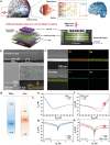
Electrical transport properties of the WSe2/InAs van der Waals (vdW) heterojunction device. a) Conceptual schematic of a retinomorphic device. b) cross‐sectional TEM images of WSe2/InAs van der Waals (vdW) heterojunction device (inset: high‐resolution TEM image), and c) corresponding elemental mapping of WSe2/InAs vdW heterojunction device, illustrating the distributions of W (orange), Se (yellow), In (green), and As (cyan). d) WSe2/InAs band structure determined from ultraviolet photoelectron spectroscopy and a Tauc plot. Transfer characteristics of the e) WSe2 and f) WSe2/InAs vdW heterojunction device in the dark and under 5 mW illumination (gate voltage: −50 to 50 V, drain voltage: 1 V). Output characteristics of the g) WSe2 and h) WSe2/InAs vdW heterojunction device in the dark and under 5 mW illumination at a gate voltage of −20 V.
Figure 3
Figure 3
Electrical transport properties of the WSe2/InAs vdW heterojunction device. a) Illustration of the WSe2/InAs vdW heterojunction device under 1060 nm laser illumination, where QDs enhance charge transfer. b) Responsivity and detectivity of the bare WSe2 and WSe2/InAs FET under 12.99 mW cm−2 (5 mW) illumination. c) Comparison of the responsivities of our device and previously reported devices. d) Response time of the WSe2/InAs vdW heterojunction device under a 5 mW laser. e) Comparison of the response times of the WSe2 and WSe2/InAs vdW heterojunction device.
Figure 4
Figure 4
Neuromorphic characteristics of the InAs/WSe2 artificial synapse device. a) Excitatory postsynaptic current (EPSC)response stimulated by 1060 nm laser illumination. b) EPSC is stimulated by a single(blue) pulse and three (red) optical pulses. c) Long‐term potentiation (LTP) of the WSe2/InAs FET with 0.5 and 0.2 Hz laser frequency at 5 mW illumination power. d) Synaptic weight of the WSe2/InAs vdW heterojunction device at 11 pulses under 5 mW illumination. Electrical programming of synaptic weights: e) paired‐pulse facilitation (PPF) indices from potentiation at various interval times and f) paired‐pulse depression (PPD) indices from depression under various interval times under 5 mW illumination.
Figure 5
Figure 5
Four optical programming synaptic weights of the WSe2/InAs synapse device. Emulation of Hebb's spike‐timing‐dependent plasticity rules using electrical pre‐ and postsynaptic pulses. a) Measurement setting values dependent on Hebbian learning rules. b) Illustration of optical pre‐spike and post‐spike at Δt > 0 and Δt < 0, respectively. c) Symmetric Hebbian, d) symmetric anti‐Hebbian, e) antisymmetric Hebbian, and f) antisymmetric anti‐Hebbian learning rules.
Figure 6
Figure 6
Short‐wavelength infrared‐triggered neuromorphic behavior and image recognition. a) Potentiation and depression properties of WSe2/InAs with gate voltages of −20 V and +20 V under 5 mW laser illumination. b) Schematic of ANN training for classification of the digit MNIST and the Fashion MNIST dataset. c) Fitting of WSe2/InAs LTP and LTD curves for simulations. d) The recognition rate of the simulated digit MNIST using experimental data. e) The recognition rate of the simulated Fashion MNIST using experimental data.

References

    1. Zrenner E., Science 2002, 295, 1022. - PubMed
    1. Li C., Du W., Huang Y., Zou J., Luo L., Sun S., Govorov A. O., Wu J., Xu H., Wang Z., Opto‐Electron. Adv. 2022, 5, 210069.
    1. Zhang J., Guo P., Guo Z., Li L., Sun T., Liu D., Tian L., Zu G., Xiong L., Zhang J., Huang J., Adv. Funct. Mater. 2023, 33, 2302885.
    1. Islam M. M., Krishnaprasad A., Dev D., Martinez‐Martinez R., Okonkwo V., Wu B., Han S. S., Bae T. S., Chung H. S., Touma J., Jung Y., Roy T., ACS Nano 2022, 16, 10188. - PubMed
    1. Zhang Z., Liu X., Zhou H., Xu S., Lee C., Small Struct. 2023, 5, 2300325.

LinkOut - more resources