. 2025 May;12(20):e2415272.
doi: 10.1002/advs.202415272. Epub 2025 Mar 4.

Laser-Enabled Fabrication of Flexible Printed Electronics with Integrated Functional Devices

Affiliations

Laser-Enabled Fabrication of Flexible Printed Electronics with Integrated Functional Devices

Wedyan Babatain et al. Adv Sci (Weinh). 2025 May.

Abstract

The demand for flexible and printed electronics in wearable and soft robotics applications has increased the need for scalable, additive manufacturing processes. However, traditional printed circuit board manufacturing involves complex, multistep processes, is limited to certain substrates, and faces challenges in integrating functional devices. Here, an additive, laser-enabled process is introduced for fabricating flexible, double-sided printed electronics leveraging laser-induced graphene (LIG) as a seed layer for selective copper electrodeposition (E-LIG). This technique enables precise conductive circuit patterning down to 50 µm and is reliable via formation in a single streamlined process. E-LIG supports transfer to various substrates, allowing for large-area electronics up to 100 cm2, broadening applications in large-scale interfaces. Functional LIG device integration, including sensors and actuators, directly interfaced with control circuits on a single substrate is demonstrated. Applications such as real-time graphical output and interactive interfacing showcase the method's versatility. E-LIG exhibits repairability for on-demand restoration of damaged circuits, enhancing durability and offering a scalable, cost-effective solution for multifunctional printed electronics.

Keywords: additive manufacturing; digital fabrication; flexible electronics; laser writing; printed electronics.


Conflict of interest statement

The authors declare no conflict of interest.

Figures

Figure 1
Figure 1
Process flow of the E‐LIG fabrication method for printed electronics. a) Schematic illustration of the full streamlined fabrication process including LIG patterning, from two sides followed by via and tab formation. After copper plating, the tabs are removed, solder paste is applied, and surface mount devices (SMDs) are assembled. b) Cross‐sectional diagram illustrating the step‐by‐step development of the PCBs. c) Photographs showing the progression on the original polyamide substrate including the intermediate and final stages of the PCB fabrication process. d) Photograph of the fully assembled and functional double‐sided flexible PCB with e) a LED on the bottom layer.
Figure 2
Figure 2
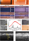
Material and physical characterization of E‐LIG traces. a) Optical images of LIG traces on polyimide showing various line widths before and b) after copper plating ranging from 50 µm to 2 mm. c) Zoomed‐in microscopic image of 500 and 100 µm thick LIG traces before and d) after copper plating demonstrating the uniformity of copper deposition across the same trace width. e) Scanning electron microscope (SEM) image of the surface of LIG trace showing its porous graphitic nature. f) SEM image of the copper‐plated LIG showing morphological changes after Cu deposition. g) Raman spectroscopy of LIG and Cu–LIG. h) Microscopic images showing a top view of the surface of LIG and i) Cu–LIG. j,k) Cross‐sectional SEM images of copper‐plated LIG layer, showing a thickness of ≈9 µm for Cu and 18 µm for LIG.
Figure 3
Figure 3
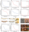
Electrical characterization of single and double‐sided E‐LIG traces as a function of process parameters. a) Resistance of LIG and b) Cu–LIG as a function of trace width. c) Resistance of Cu–LIG over time during the plating process. d) Resistance of Cu–LIG as a percentage of the original LIG resistance as a function of plating voltage, illustrating the optimal voltage range. e) Resistance of LIG and f) Cu–LIG as a function of laser power. g) Schematic of the process flow for creating double‐sided PCBs, including the LIG patterning, via formation, and Cu deposition to establish interconnections between layers. h) 3D illustration of the process of formation of LIG vias and the subsequent copper plating to create conductive paths between the two sides of the PCB. i) Microscopic images of the LIG vias before and after copper plating, showing the formation of reliable Cu electrical connections in double‐sided PCBs. j) Resistance of LIG and k) Cu–LIG as a function of via diameter. l) Photographs showing a fully Cu‐plated double‐sided trace enabled by the formation of LIG vias, with insets showing zoomed‐in views of the vias on both sides.
Figure 4
Figure 4
Fabrication and transfer of printed circuits onto transparent and large‐area substrates. a) Process flow illustration of the step‐by‐step process for transferring a fully plated and assembled PCB onto a PDMS substrate. b) Sequence of photographs showing the intermediate and final stages of the PCB transfer process. c,d) Photographs of the transferred PCB on PDMS showing the uniformity of the transfer process and the flexibility of the transferred PCB on PDMS. e,f) A large‐area (10 cm × 10 cm) LED matrix fabricated on using the E‐LIG method, demonstrating the scalability of the process. g) Transferred PCB on PDMS integrated with a LIG resistive sensor controlling the brightness of a LED, showing seamless functional integration.
Figure 5
Figure 5
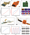
E‐LIG integrated electronics for sensor applications. a) Schematic illustration of the layer‐by‐layer fabrication process of E‐LIG board with integrated functional LIG strain sensor. b) Schematic and c) photograph of the strain sensing integrated system including the sensing element and its readout circuit in one substrate. d) Correlation of the resistance of the sensing element with the overall strain applied from 5% to 25%. e) Resistance of the sensor during a cyclic test of 10 repeated strain cycles at various strain values. f) Schematic representing the integrated LIG pressure sensor, including the pressure‐sensitive element and readout circuit. g) Schematic showing how external pressure is applied to the sensor, causing a change in resistance due to its piezoresistive behavior. h) Layout of the readout circuit designed for sensor interface. i) Physical image of the integrated LIG‐based pressure sensor system. j) The resistance–pressure characteristic curve demonstrates a linear increase in resistance as pressure increases. k) Dynamic resistance response of the sensor under multiple increasing pressure cycles.
Figure 6
Figure 6
E‐LIG integrated electronics for actuator applications. a) Schematic illustration of the E‐LIG fabricated board with an integrated thin‐film LIG heater. b) Photograph of the LIG‐based heater integrated with its control circuit on the same substrate. c) Layout of the circuit design for the heater interface and control. d) Temperature versus voltage characteristics of the heater show an increase in temperature with increasing voltage. e) Dynamic response of the heater during incremental voltage steps. f) Infrared thermal images showing the temperature distribution across the LIG heater at different voltages. g) Schematic of the LIG‐based electrothermal actuator integrated with an E‐LIG board. h) Photograph of the LIG‐based electrothermal actuator integrated system. i) Bending angle of the actuator as a function of the applied voltage. j) Dynamic actuation response of the LIG‐based actuator under cyclic voltage application driven by a 50 V square wave. k) Sequential images showing the physical bending of the electrothermal actuator at different applied voltages (0–60 V).

References

    1. Gao W., Ota H., Kiriya D., Takei K., Javey A., Acc. Chem. Res. 2019, 52, 523. - PubMed
    1. Corzo D., Blazquez G. T., Baran D., Front. Electron. 2020, 1, 594003.
    1. Khan Y., Thielens A., Muin S., Ting J., Baumbauer C., Arias A. C., Adv. Mater. 2020, 32, 1905279. - PubMed
    1. El‐Atab N., Mishra R. B., Al‐Modaf F., Joharji L., Alsharif A. A., Alamoudi H., Diaz M., Qaiser N., Hussain M. M., Adv. Intell. Syst. 2020, 2, 2000128.
    1. Hussain M. M., El‐Atab N., Handbook of Flexible and Stretchable Electronics, CRC Press, Boca Raton, FL: 2019.

LinkOut - more resources