. 2025 Mar 19;25(11):4401-4407.
doi: 10.1021/acs.nanolett.4c06545. Epub 2025 Mar 10.

Attojoule Superconducting Thermal Logic and Memories

Affiliations

Attojoule Superconducting Thermal Logic and Memories

Hui Wang et al. Nano Lett. .

Abstract

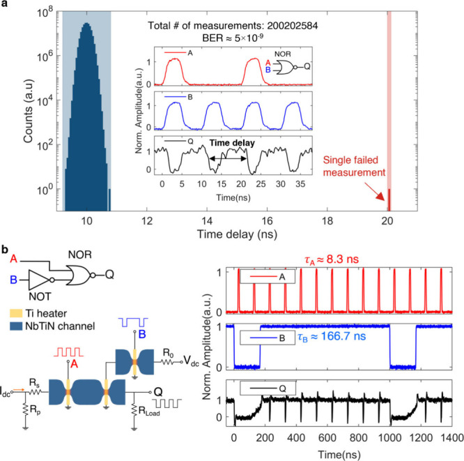
Due to stringent thermal budgets in cryogenic technologies such as superconducting quantum computers and sensors, electronic building blocks that simultaneously offer low energy consumption, fast switching, low error rates, a small footprint, and simple fabrication are pivotal for large-scale devices. Here, we demonstrate a superconducting switch with attojoule switching energy, high speed (pico-second rise/fall times), and high integration density (on the order of 10-2 μm2 per switch). It consists of a superconducting nanochannel and a metal heater separated by an insulating silica layer. We experimentally demonstrate digital gate operations utilizing these nanostructures, such as NOT, NAND, NOR, AND, and OR gates, with a few femtojoules of energy consumption and ultralow bit error rates <10-8. In addition, we build energy-efficient volatile memory elements with nanosecond operation speeds and a retention time over 105 s. These superconducting switches open new possibilities for increasing the size and complexity of modern cryogenic technologies.

Keywords: Superconducting device; digital circuits; logic gate; memory device.


Conflict of interest statement

The authors declare no competing financial interest.

Figures

Figure 1
Figure 1
Characterization of the superconducting thermal switch. a, Schematic picture and b, scanning electron microscopy image of the superconducting thermal switch consisting of a NbTiN channel covered by a layer of silica and a metal heater. c, The device switches between the superconducting (“On”) state and the resistive (“Off”) state due to heat transfer from the metal layer via the silica to the NbTiN channel. d, Resistance of the NbTiN channel (RNbTiN) as a function of the bias current (Ib) and the current through the metal heater (Ih).
Figure 2
Figure 2
a, Schematic of the experimental circuit to test the transient response of the superconducting thermal switch. b, Voltage traces of a superconducting thermal switch with a clock input signal. Note: signal attenuations and amplifications have been accounted for, and the corrected curves are plotted (see Supporting Information section 2 for more details). The input signal is a 10 MHz square wave with a pulse duration τh ≈ 4.2 ns and an amplitude Vh ≈ 7.2 mV. The device is biased with Ib = 28.5 μA, and the metal heater has a resistance Rh = 291.5 Ω.
Figure 3
Figure 3
Construction of fundamental logic gates. a-c, Implementation of fundamental logic gates NOT (a), NOR (b), and NAND (c) using superconducting thermal switches. Figures on the left are the schematic diagrams. Figures on the right are the corresponding experimental waveforms of the inputs (A, B) and output (Q), rescaled according to the logic HIGH and LOW levels. The resistive elements shown in the figures are R0 = 22 Ω, RLoad = 50 Ω, Rp = 100 Ω, and Rs = 50 Ω.
Figure 4
Figure 4
Bit error rate (BER) and driving ability of the logic gates. a, Correct (blue) and incorrect (red) operations of a NOR gate over 2 × 10⁸ measurements as used to calculate the bit error rate (BER). The inset displays typical input (A: 50 MHz with a pulse duration of 4.2 ns, B: 100 MHz with a pulse duration of 4.2 ns) and output signals (Q) of the NOR gate. The horizontal coordinate represents the time delay between the falling edges of two consecutive pulses at the output, which was triggered at 50% of the output pulse amplitude. b, Electrical diagram (left) and experimental results (right) of a simple logic circuit composed of a NOT gate and a NOR gate.
Figure 5
Figure 5
Memory operations of a superconducting thermal switch. a, Use of the superconducting thermal switch as a memory cell. b, Circuit diagram (top) and experimental characteristics (bottom) of the memory. The output Q is amplified by an AC-coupled amplifier (50 Ω input impedance). R1 = 22 Ω and R2 = 50 Ω are chosen for better impedance matching. Basic memory operations (bottom) are denoted as W for Write, RS for Reset, and R for Read (“0” for reading a superconducting state, where an output pulse is captured, and “1” for reading a resistive state, where no output signal is observed). c, Read operation of the state “0” with a subnanosecond input pulse. The output pulse has a fwhm of around 550 ps. d, Measurement of the BER based on the output voltage difference ΔV between “0” and “1” state. The 4 incorrect measurements are marked in red, and correct measurements in blue. The total number of measurements is five million, leading to a BER of 8 × 10⁻⁷.

References

    1. Berggren K. Quantum Computing with Superconductors. Proceedings of the IEEE 2004, 92, 1630–1638. 10.1109/JPROC.2004.833672. - DOI
    1. Wu Y.; et al. Strong Quantum Computational Advantage Using a Superconducting Quantum Processor. Phys. Rev. Lett. 2021, 127, 180501.10.1103/PhysRevLett.127.180501. - DOI - PubMed
    1. Sobolewski R.; Verevkin A.; Gol’tsman G. N.; Lipatov A.; Wilsher K. Ultrafast superconducting single-photon optical detectors and their applications. IEEE Transactions on Applied Superconductivity 2003, 13, 1151–1157. 10.1109/TASC.2003.814178. - DOI
    1. Toomey E.; et al. Superconducting Nanowire Spiking Element for Neural Networks. Nano Lett. 2020, 20, 8059–8066. 10.1021/acs.nanolett.0c03057. - DOI - PubMed
    1. Khan S.; et al. Superconducting optoelectronic single-photon synapses. Nature electronics 2022, 5, 650–659. 10.1038/s41928-022-00840-9. - DOI

LinkOut - more resources