. 2025 May;21(18):e2410841.
doi: 10.1002/smll.202410841. Epub 2025 Mar 24.

Synergistically Engineered All Van der Waals GaS-WSe2 Photodiodes: Approaching Near-Unity Polychromatic Linearity for Multifunctional Optoelectronics

Affiliations

Synergistically Engineered All Van der Waals GaS-WSe2 Photodiodes: Approaching Near-Unity Polychromatic Linearity for Multifunctional Optoelectronics

Tawsif Ibne Alam et al. Small. 2025 May.

Abstract

Van der Waals (vdW) heterojunctions represent a significant frontier in post-Moore era optoelectronics, especially in optimizing photosensor performance through multivariate approaches. Here synergistic engineering of GaS-WSe2 all-vdW photodiodes is investigated, which exhibit broadband detection (275-1064 nm), multispectral unity approaching linearity, alongside a substantial linear dynamic range (LDR) of 106.78 dB. Additionally, the photodiodes achieve a remarkable on/off ratio of 105 and rapid response edges of 545/471 µs under a 405 nm pulsed source, exhibiting ultralow light detection capabilities (dark currents ∼fA), culminating in a peak responsivity of 376.78 mA W-1 and a detectivity of 4.12 × 10¹¹ Jones under 450 nm illumination, complemented by an external quantum efficiency (EQE) of 30% and a fill factor of ≈0.33. Based on the analysis of multiple all-vdW devices, the importance of Fermi-level pinning free metal-2D interface engineering that enables effective modulation of the Schottky barrier height via vdW metal contacts is highlighted and meticulous thickness-engineered layers in developing a robust depletion region within the type-II GaS-WSe2 heterojunction are employed, ultimately achieving a favorable balance among photocarrier generation recombination, separation, transport, and extraction. This comprehensive investigation sets the stage for future developments in critically engineered next-generation vdW optoelectronic devices.

Keywords: Fermi‐level pinning; GaS–WSe2 heterostructure; all van der Waals; broadband photodiode; photovoltaic; type‐II heterojunction; van der Waals contact.


Conflict of interest statement

The authors declare no conflict of interest.

Figures

Figure 1
Figure 1
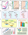
a) Schematic Illustration of all van der Waals heterojunction photodetector (purple and red spheres represent gallium and tungsten metal atoms, while blue and yellow spheres represent sulfur and selenium atoms, respectively). b) Optical microscopic image of the device. c) Raman spectroscopy of few‐layer GaS showing characteristics A1 1g, E1 2g, and A2 1g modes, ultrathin WSe2 showing characteristics E1 2g and A1g modes, and the heterojunction region showing all the characteristics peaks. d) Raman mapping of A1g mode (256.94 cm−1) of WSe2 (top) and A2 1g (359.58 cm−1) of GaS, showing evident uniform Raman quenching in the overlapped regions for both the modes. e) Photoluminescence spectroscopy of ultrathin WSe2 in the bare and overlapped regions of the heterojunction, with the inset showing the PL mapping. Evident PL quenching is observed from both the spectroscopy and mapping results.
Figure 2
Figure 2
a) AFM image of the heterojunction region with corresponding height profiles showing a thickness of GaS and WSe2 layer of 8.5 nm (region A) and 3 nm (region B), respectively. b) KPFM image of the heterojunction region with the corresponding SPD profile, showing an SPD of ≈200 mV. c) Cross‐sectional HR‐STEM image of the all‐vdW region of the heterojunction, showing (from bottom) h‐BN, WSe2, GaS, and vdW contact, with pristine interfaces between constituent junctions.
Figure 3
Figure 3
a) Dark I dV d profile of the photodiode, showing two distinct linear regions with ideality factor η 1 and η 2 of 1.6 and 2.96, respectively. b) ln (I d/V d 2) versus 1/V d plot of the diode forward current regime, showing three distinct operation regions (DT, FN, and SPLC). c) Double log I dV d plot of the forward current. d) Schematic illustration of transport characteristics of the photodiode under forward and reverse bias conditions. e) Pseudoband potential of the heterojunction under quasiequilibrium state of illumination, illustrating intralayer transitions (T 1 and T 2) and interlayer transition (T 3). f) Proposed layer‐dependent evolution of conduction band profile of GaS with respect to silver contact. g) Strategy for optimization of WSe2 layers for efficient charge generation, separation, and extraction.
Figure 4
Figure 4
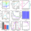
Optoelectronic characteristics of the device under 450 nm illumination. a) Evolution of log I dV d characteristics under increased illumination power. b) Zoomed region of I dV d showing clear I SC and V OC. c) I SC and V OC versus power density plot showing a linear region for I SC and no saturation with an LDR of 106.7 dB and V OC saturation at 0.36 V. d) Electrical power characteristics of the photodiode under increased illumination showing various PCE under varied illumination conditions. e) Responsivity and detectivity versus power density of the device, showing a peak photovoltaic responsivity of 376.76 mA W−1 and a detectivity of 4.12 × 10¹¹ Jones. Temporal photocurrent response of the device at 405 nm illumination, showing f) 200 cycles of switching stability with no degradation, g) evolution of stability of the device under a course of 90 days observation period, h) rise and fall times of the device showing 545 µs (rise) and 471 µs (fall) edges, and i) frequency response showing a cutoff (−3 dB) at 697 Hz.
Figure 5
Figure 5
a) Photovoltaic temporal response of the device under maximum available illumination conditions of the device under various wavelengths. The device shows a photovoltaic response between 275 and 1064 nm, with a peak on–off ratio of 105. b) Evolution of PCE of the fabricated a‐vdW devices, suggesting the need for synergistic thickness engineering for efficient light‐harvesting characteristics, with a maximum PCE for synergistically optimized device‐1 and minimum for device‐2 having a thicker GaS and WSe2 regions, with intermediate performance from device‐3, constructed from ultrathin WSe2, similar to device‐1 and slightly thicker GaS than device‐1. c) Comparison of responsivity and detectivity for the fabricated devices under similar illumination conditions at 405 nm. d) Comparison of rise/fall time and power exponent of all the fabricated devices under 405 nm illumination.
Figure 6
Figure 6
a) Schematic illustration of a single‐pixel imaging system. b) Reconstructed image of the pattern “P O L Y U.” c) Variation of V OC, with tuned V g, under illumination at 405 nm. A state of high (V OC > 0.35 V) and low (V OC < 0.15) could be outlined in the sky blue and pink regions, respectively. d) Schematic illustration of the optoelectronic logic AND gate (top) and its corresponding state table (bottom). e) State trace and corresponding logic function demonstration of the optoelectronic AND operation.

References

    1. Britnell L., Ribeiro R. M., Eckmann A., Jalil R., Belle B. D., Mishchenko A., Kim Y.‐J., Gorbachev R. V., Georgiou T., Morozov S. V., Grigorenko A. N., Geim A. K., Casiraghi C., Castro Neto A. H., Novoselov K. S., Science 2013, 340, 1311. - PubMed
    1. Wong J., Jariwala D., Tagliabue G., Tat K., Davoyan A. R., Sherrott M. C., Atwater H. A., ACS Nano 2017, 11, 7230. - PubMed
    1. Hu P., Wang L., Yoon M., Zhang J., Feng W., Wang X., Wen Z., Idrobo J. C., Miyamoto Y., Geohegan D. B., Xiao K., Nano Lett. 2013, 13, 1649. - PubMed
    1. Chitara B., Ya'Akobovitz A., Nanoscale 2018, 10, 13022. - PubMed
    1. Araujo F. D. V., Oliveira V. V., Gadelha A. C., Carvalho T. C. V., Fernandes T. F. D., Silva F. W. N., Longuinhos R., Ribeiro‐Soares J., Jorio A., Souza Filho A. G., Alencar R. S., Viana B. C., Nanotechnology 2020, 31, 495702. - PubMed

LinkOut - more resources