. 2021 Oct 19;2(1):2100047.
doi: 10.1002/smsc.202100047. eCollection 2022 Jan.

Chemical Vapor Deposition Mediated Phase Engineering for 2D Transition Metal Dichalcogenides: Strategies and Applications

Affiliations

Chemical Vapor Deposition Mediated Phase Engineering for 2D Transition Metal Dichalcogenides: Strategies and Applications

Karla Hernandez Ruiz et al. Small Sci. .

Abstract

2D transition metal dichalcogenides (TMDs) are characterized by the presence of multiple crystal structures or phases, even at the ultrathin limit. Controlling phase transformations, namely, phase engineering, of 2D TMDs is crucial for realizing high-performance 2D devices by combining phases with distinct physical and chemical properties. As a powerful approach for large-scale production of high-quality 2D TMDs, chemical vapor deposition (CVD) offers unique advantages in phase engineering due to its highly controllable synthesis processes. Starting with an introduction of the crystal structures and phase transformations of 2D TMDs, this review summarizes the recent developments in CVD-mediated phase engineering strategies of TMDs, including control of temperature, precursors, catalysis, atmosphere, composition, and strain during the deposition process. Moreover, the representative applications of CVD-based phase-engineered TMDs in the field of transistors, photodetectors, photovoltaic cells, and catalysis are overviewed. Finally, the challenges, expectations of CVD-based phase engineering, and future development of this versatile technique are discussed.

Keywords: 2D transition metal dichalcogenides; chemical vapor deposition; phase-selective growth.


Conflict of interest statement

The authors declare no conflict of interest.

Figures

Figure 1
Figure 1
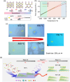
Scheme of the characteristic CVD setup for 2D TMDs growth and the approaches to CVD‐mediated phase engineering.
Figure 2
Figure 2
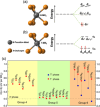
Schematic illustration of the metal coordination, basal plane, and side view of a) 2H and 3R, b) 1T, and c) 1T′ and Td phases of TMDs. The basal plane and side view of every phase are also exhibited.
Figure 3
Figure 3
a) Splitting of the 3d orbital energy levels of a trigonal prismatic (H phase) and b) octahedral (T phase) crystal field. Electron filling of group 6 TMDs is shown as an example. c) Stress‐free (zero stress, σ) energy difference among phases of monolayer TMDs. Because σ = 0, Energy U is equivalent to the enthalpy H. TMDs as classified by its transition metal group. a,b) Reproduced with permission.[ 31 ] Copyright 2017, IOP Publishing Ltd. c) Illustration of the data presented in Ref. [31].
Figure 4
Figure 4
Band structures of MoTe2 polytypes. a–c) 2H, 1T′, and Td phases. d,e) Enlarged images close to the Fermi level (E F) for (d) 1T′ and c) Td. a–e) Reproduced with permission.[ 126 ] Copyright 2016, American Chemical Society.
Figure 5
Figure 5
a) A STEM‐ADF image taken at the phase boundary (dashed line). The left and right domains present the 2H and 1T phases of MoS2, respectively. FFT patterns of b) 2H and c) 1T MoS2. d) The ADF intensity profile taken from the green area in (a). The intensity profile taken at the blue line is placed on the image which width corresponds to 3.9 nm. a–d) Reproduced with permission.[ 36 ] Copyright 2012, American Chemical Society. e) Structure model and f) HAADF image of 1T′ phase MoS2, showing three different Mo—Mo distances with clear Mo—Mo zig—zag chains. e,f) Reproduced with permission.[ 127 ] Copyright 2017, Royal Society of Chemistry.
Figure 6
Figure 6
a) Raman spectra of 1T and 2H phases of MoS2 measured by a 532 nm laser. Reproduced with permission.[ 41 ] Copyright 2020, National Academy of Sciences. b) Raman spectra of 2H and 1T′ phases of MoTe2 measured by a 532 nm laser. Reproduced under the terms of the CC‐BY 4.0 license.[ 44 ] Copyright 2020, The Authors, published by Springer Nature. c) XPS analysis of Mo 3d, S 2s, and S 2p core levels of samples annealed at different temperatures. The deconvolution shows the contributions of 2H and 1T of MoS2 phases represented in red and green, respectively. Reproduced with permission.[ 46 ] Copyright 2011, American Chemical Society.
Figure 7
Figure 7
Schematic illustration of the a) one‐step and b) two‐step route for the deposition of 2D TMDs by CVD.
Figure 8
Figure 8
a) Schematic illustration of the CVD setup for MoTe2 and the phases obtained by different quenching temperatures. b) Free energy of 1T, 1T′, and 2H phases of MoTe2 against temperature plot. a,b) Reproduced with permission.[ 48 ] Copyright 2016, American Chemical Society. c) Optical images of MoTe2 films deposited at different temperatures deposited at between 600 and 800 °C. Reproduced with permission.[ 50 ] Copyright 2019, American Chemical Society. d) Schematic illustration of the reverse flow CVD process for the deposition of bilayer MoS2. Reproduced under the terms of the CC‐BY 4.0 license.[ 53 ] Copyright 2019, The Authors, published by Springer Nature.
Figure 9
Figure 9
a) Effect of the deposition parameters on the synthesis of 3R‐MoS2. The results were obtained at different furnace center temperatures and MoCl5 temperatures at the furnace center and edge. Reproduced with permission.[ 58 ] Copyright 2018, Wiley‐VCH. b) Graph of the phase evolution of MoTe2 as a function of the carrier gas flow rate. c) Raman analysis of different MoTe2 films grown at different N2 flow rates. b,c) Reproduced with permission.[ 22 ] Copyright 2017, American Chemical Society.
Figure 10
Figure 10
a) Energy shift of WTe2x S2(1–x) alloy versus concentration of Te (x). b) Raman spectra of WTe2x S2(1–x) alloys with x = 0, 0.04, 0.08, 0.12, 0.16, 0.2, and 0.85, respectively. a,b) Reproduced with permission.[ 68 ] Copyright 2019, Wiley‐VCH. c) HAADF intensity histograms of metal and chalcogenide sites showing that Re% is 22.9%, confirming a 2H phase. d) Atom labeled image presenting Re doping with uniform distribution. c,d) Reproduced with the permission.[ 69 ] Copyright 2017, Wiley‐VCH.
Figure 11
Figure 11
a) Optical images and Raman spectra obtained from samples prepared with 1) 50 sccm, 2) 200 sccm, 3) 250 sccm, 4) 300 sccm, 5) 500 sccm, and 6) 700 sccm of H2. The green and yellow scale bars represent 2 and 5 μm, respectively. Reproduced with permission.[ 73 ] Copyright 2019, American Chemical Society. b) Phase diagram of WS2(1−x)Te2x alloys with Te% as function of the H2 gas flow. c–d) HAADF‐STEM images of alloys with 2H and 1T′ phases, respectively. Insets show the FFT patterns from the 2H and 1T′ phases. b–d) Reproduced with permission.[ 74 ] Copyright 2019, Elsevier B.V.
Figure 12
Figure 12
a) Schematic representation of CVD grown 1T′ MoTe2 assisted by molecular sieves. Reproduced with permission.[ 77 ] Copyright 2020, The Royal Society of Chemistry. b) SEM image of a butterfly‐like WS2 flake with an ADF image taken in the grain boundary of different phases. Reproduced with permission.[ 78 ] Copyright 2018, American Chemical Society. c) Schematic illustration of the CVD process for the synthesis of 1T TaS2. d) TaS2 precursor:KCl ratio versus percentage of 1T TaS2 diagram. c,d) Reproduced with permission.[ 79 ] Copyright 2019, The Royal Society of Chemistry.
Figure 13
Figure 13
a) Schematic representation of the CVD setup used for the synthesis of Mo1−x W x S2. An electric fan was used to induce fast cooling in the sample, when the fan was not used the cooling was slow. b) Graph of 1T phase proportion versus thermal strains from different substrates. c) XPS results of the Mo1−x W x S2 films grown on glass at 700 °C followed by an annealing process at 500 °C while on the substrate, or a free‐standing annealing at 500 °C. The terms “Fst.,” “slw.,” “on‐sub.,” “free‐sta.,” and “annl.” are assigned to “fast cooling,” “slow cooling,” “on‐substrate,” “free‐standing,” and “annealing,” respectively. a–c) Reproduced with permission.[ 81 ] Copyright 2018, American Chemical Society.
Figure 14
Figure 14
Schematic illustration of electronic, optoelectronic, and electrocatalytic applications for CVD phase‐engineered 2D TMDs.
Figure 15
Figure 15
Phase‐engineered 2D TMD‐based FET devices. a) Electrostatic force microscopy image of a MoS2 nanosheet shows different phases, 2H phase presents bright color, and 1T phase exhibits dark color. b,c) Output characteristics devices with Au and 1T MoS2 electrodes, respectively. V ds = 5 V and V gs goes from −10 to 30 V. a–c) Reproduced with permission.[ 5 ] Copyright 2014, Springer Nature. d) Optical image of ≈1500 devices synthesized in a centimeter scale. e) SEM image of the MoTe2 device with 2H MoTe2, 1T′ MoTe2, and WTe2 represented by yellow, green, and blue colors, respectively. The inset is an optical image of the device. f) Optical image of a representative MoTe2 FET with a CNT gate. d–f) Reproduced with permission.[ 57 ] Copyright 2019, Springer Nature. g) Optical images of a 1T′/2H/1T′ MoTe2 device and its connections. h) Room temperature I − V characteristics of different connection pairs. g,h) Reproduced with the permission.[ 87 ] Copyright 2017, American Chemical Society.
Figure 16
Figure 16
Phase‐engineered 2D TMDs based DSSC devices. a) Cross‐sectional SEM images of CE heterostructures. b) Schematic representation of the DSSC device using a WS2/MoTe2 CE. c) J—V curves of all electrodes including Pt at 100 mW cm−2 light intensity. Three thicknesses of the WS 2 layer were prepared as ≈119, ≈203, and ≈273 nm, and the samples were denoted as S1, S2, and S3, respectively. The thickness of MoTe2 film was fixed at ≈350 nm. a–c) Reproduced with permission.[ 93 ] Copyright 2018, Royal Society of Chemistry. d) SEM images of Mo x W1–x Te2 nanoflakes grown on CC. e) Electrochemical impedance spectroscopy for all CE. f) J—V curves for all CE at 100 mW cm−2 solar illumination. d–f) Reproduced with permission.[ 49 ] Copyright 2019, Wiley‐VCH.
Figure 17
Figure 17
Phase‐engineered 2D TMD‐based photodetector and photovoltaic devices. a) Source—drain bias voltage versus responsivity of 1T′ and 2H MoTe2 photodetectors. Reproduced with permission.[ 100 ] Copyright 2019, Elsevier B.V. b) Optimal image of the MoTe2/MoS2 heterostructures. c) Responsivity of the MoTe2/MoS2 heterostructures at different incident light from 300 to 1000 nm. d) I—V curves of the heterostructures illuminated with different wavelength lasers and in the dark. b–d) Reproduced with permission.[ 101 ] Copyright 2018, Elsevier B.V. e) Schematic representation of the Mo x Re1–x S2 device. f) Optical microscope image of Mo x Re1–x S2 device. g) Bandgap as a function of the Mo composition (x). h) Photocurrent as a function of time for ReS2, MoS2, and Mo x Re1–x S2 under light illumination with different wavelengths. e–h) Reproduced with permission.[ 103 ] Copyright 2020, Wiley‐VCH.
Figure 18
Figure 18
Phase‐engineered 2D TMD‐based HER electrocatalysts. a) SEM image of the MoS2@NPG material. b) Polarization curves of platinum, NPG, and MoS2@NPG samples. c) Corresponding Tafel slopes. a–c) Reproduced with permission.[ 118 ] Copyright 2014, Wiley‐VCH. d) SEM image of the film‐like 1T′ MoTe2 deposited on CC. e) Polarization curves corresponding to all electrocatalyst where the letters F, P, LG, and SG refer to film‐like, porous, large granular, and small granular morphologies, respectively. f) The Gibbs free energies of H‐adsorption of different MoTe2 phases. d–f) Reproduced with permission.[ 94 ] Copyright 2019, American Chemical Society.

Similar articles

Cited by

References

    1. Novoselov K. S., Geim A. K., Morozov S. V., Jiang D., Zhang Y., Dubonos S. V., Grigorieva I. V., Firsov A. A., Science 2004, 306, 666. - PubMed
    1. Mas-Ballesté R., Gómez-Navarro C., Gómez-Herrero J., Zamora F., Nanoscale 2011, 3, 20. - PubMed
    1. a) Liu Y., Duan X., Huang Y., Duan X., Chem. Soc. Rev. 2018, 47, 6388; - PubMed
    2. b) Glavin N. R., Rao R., Varshney V., Bianco E., Apte A., Roy A., Ringe E., Ajayan P. M., Adv. Mater. 2020, 32, 1904302; - PubMed
    3. c) Duong D. L., Yun S. J., Lee Y. H., ACS Nano 2017, 11, 11803. - PubMed
    1. a) Bertolazzi S., Bondavalli P., Roche S., San T., Choi S.-Y., Colombo L., Bonaccorso F., Samorì P., Adv. Mater. 2019, 31, 1806663; - PubMed
    2. b) Xia F., Wang H., Xiao D., Dubey M., Ramasubramaniam A., Nat. Photonics 2014, 8, 899;
    3. c) Liang S.-J., Cheng B., Cui X., Miao F., Adv. Mater. 2020, 32, 1903800; - PubMed
    4. d) Zhu W., Low T., Wang H., Ye P., Duan X., 2D Mater. 2019, 6, 032004;
    5. e) Meng C., Das P., Shi X., Fu Q., Müllen K., Wu Z.-S., Small Sci. 2021, 1, 2000076.
    1. Kappera R., Voiry D., Yalcin S. E., Branch B., Gupta G., Mohite A. D., Chhowalla M., Nat. Mater. 2014, 13, 1128. - PubMed

LinkOut - more resources