. 2023 Aug 17;3(9):2300100.
doi: 10.1002/smsc.202300100. eCollection 2023 Sep.

1 nm-Resolution Sorting of Sub-10 nm Nanoparticles Using a Dielectric Metasurface with Toroidal Responses

Affiliations

1 nm-Resolution Sorting of Sub-10 nm Nanoparticles Using a Dielectric Metasurface with Toroidal Responses

Hong Luo et al. Small Sci. .

Abstract

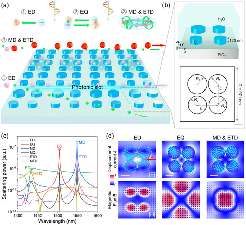
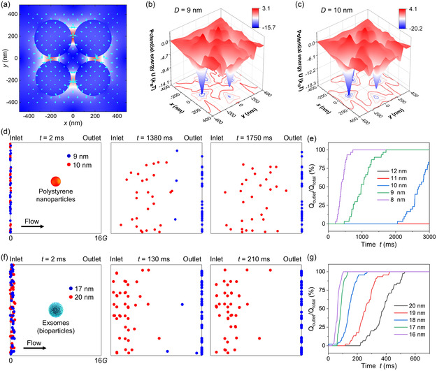
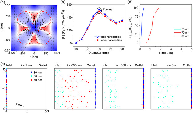
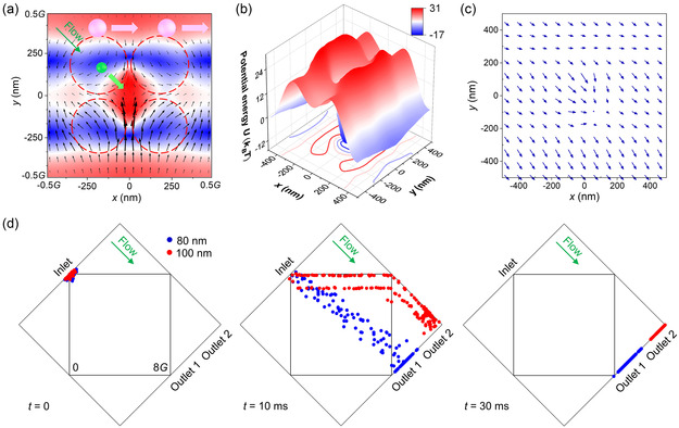
Sorting nanoparticles is of paramount importance in numerous physical, chemical, and biomedical applications. Current technologies for sorting dielectric nanoparticles have a common size limit and resolution approximately of 20 and 10 nm, respectively. It remains a grand challenge to push the limit. Herein, the new physics that deploys toroidal and multipole responses in a dielectric metasurface to exert strong and distinguishable optical forces on sub-10 nm nanoparticles is unravelled. The electric toroidal dipole, electric dipole, and quadrupole emerge with distinct light and force patterns, which can be leveraged to promise unprecedented high-precision manipulations, such as sorting sub-10 nm polystyrene nanoparticles at 1 nm resolution, sorting 20 nm proteins/exsomes at 3 nm resolution, conveying, and concentrating 100 nm gold nanoparticles. Remarkably, the design can also be employed to screen out medium-sized nanoparticles from a mixture of nanoparticles with over three sizes. This optofluidic manipulation platform opens the new way to explore intriguing optical modes for the powerful manipulation of nanoparticles with nanometer precisions and low laser powers.

Keywords: 1 nm resolution; dielectric metasurface; optofluidic sorting; sub-10 nm nanoparticles; toroidal dipole.


Conflict of interest statement

The authors declare no conflict of interest.

Figures

Figure 1
Figure 1
Electric and magnetic dipoles and multipoles for multifunctional and high‐precision manipulation of nanoparticles. a) Schematics of the ETD, ED, and EQ emerged by the illuminating a nanopillar array using a normally incident plane wave with the electric field along the x direction. With the ETD, medium‐sized nanoparticle can be trapped inside hotspots, while other nanoparticles flushed away by the flow stream. With the ED, nanoparticles can be sorted and pushed along a photonic slot. b) Structural parameters of a unit cell consisting of four silicon pillars on a silicon oxide substrate. The nanopillars have a height of 120 nm and are imbedded in water. Two nanopillars in the upper low have a radius R 1 = 170 nm; the other two in the lower low have a radius R 2 = 160 nm. The distance between two nanopillars L = 360 nm, and the length of each unit cell G = 971 nm. c) Multipole expansion. ED, electric dipole; MD, magnetic dipole; EQ, electric quadrupole; MQ, magnetic quadrupole; ETD, electric toroidal dipole; MTD, magnetic toroidal dipole. d) Analysis of different optical modes by plotting the displacement current and magnetic flux. The normalized electric and magnetic fields are plotted at z = 60 nm. Scale bars equal 200 nm.
Figure 2
Figure 2
High‐resolution sorting of polystyrene nanoparticles and exsomes at the wavelength of 1550 nm. a) Plot of the electric field and force vectors on a 10 nm polystyrene (RI = 1.58) nanoparticle for the ETD mode. The four electric hotspots exert optical gradient forces on the nanoparticle. b,c) Potential wells for 9 nm (b) and 10 nm (c) polystyrene nanoparticles. I = 10 mW μm−2 in (b) and (c). d) Simulated video frames of sorting of 9 and 10 nm polystyrene nanoparticles. All 10 nm nanoparticles reach the outlet on the right side at t = 1.75 s, while no 9 nm nanoparticles reach the outlet at that time. The separation of the two kinds of nanoparticles can be prominent when we enlarge the working range to, for example, 100 μm. e) Quantified percentage of 8–12 nm polystyrene nanoparticles to the outlet with time. f) Simulated video frames of sorting of 17 and 20 nm exsomes. All 17 nm nanoparticles reach the outlet on the right side at t = 210 s, while no 20 nm nanoparticles reach the outlet at that time. g) Quantified percentage of 16–20 nm exsomes to the outlet with time. In (d) and (e), I = 19 mW μm−2, v = 80 μm s−1. In (f) and (g), I = 9.5 mW μm−2, v = 300 μm s−1.
Figure 3
Figure 3
Screening medium‐sized nanoparticles from a bunch of nanoparticles using an ultralow laser intensity (0.036 mW μm−2) at the wavelength of 1550 nm. a) Plot of the electric field and Poynting vector of the ETD mode at z = 150 nm. The four electric hotspots tend to trap nanoparticles inside by the optical gradient force, while Poynting vectors tend to push away nanoparticles by the radiation pressure. The potential well depth thus comes from the competition of two forces. The electric field and Poynting vectors are plotted at a plane 30 nm above the substrate. b) Potential well depth |U| versus the diameter of nanoparticle. In the range of 10–90 nm, for both gold and silver nanoparticles, |U| initially increases and then drops with the particle size at a turning point of 50 nm due to the large radiation pressure on big nanoparticles. Thus, we can only trap 50 nm nanoparticles and release 30 and 70 nm nanoparticles by controlling the laser power and flow velocity. c) Video frames of the screening 50 nm polystyrene nanoparticles from 30 and 70 nm ones. 30 nm (blue) and 70 nm (red) nanoparticles successively move to the outlet on the right side by the fluidic drag force. In contrast, 50 nm nanoparticles are trapped inside hotspots in the flow stream. I = 0.036 mW μm−2, and v = 50 μm s−1. d) Quantified percentage of nanoparticles to the outlet with time. 30 and 70 nm nanoparticles move to the outlet in 0.6 and 1.8 s, respectively.
Figure 4
Figure 4
Fast sorting and transporting of gold nanoparticles by the photonic slot in the electric dipole mode at the wavelength of 1435.6 nm. a) Plot of the electric field and Poynting vector of the ED mode at z = 150 nm. When implementing a tilted flow stream, the small nanoparticle (green) is carried away by the flow stream, while the large nanoparticle (pink) is confined in the photonic slot by the optical gradient force and transported by the fluidic drag force in the x direction. b) Potential well of the 80 nm gold nanoparticle. A photonic slot and a hole occur in the edge and in the middle of a unit cell, respectively. c) Plot of the total force (optical force + fluidic drag force) on an 80 nm gold nanoparticle. d) Video frames of sorting and transporting gold nanoparticles. 80 nm gold nanoparticles (blue) move along the fluidic drag force, while 100 nm gold nanoparticles (red) are confined in photonic slot and transported by the fluidic drag force in the x direction. In (b−d), I = 2.1 mW μm−2, and v = 1500 μm s−1.

Similar articles

References

    1. De M., Ghosh P. S., Rotello V. M., Adv. Mater. 2008, 20, 4225.
    1. Lu A.-H., Salabas E. L., Schüth F., Angew. Chem., Int. Ed. 2007, 46, 1222. - PubMed
    1. Chen X., Lv H., NPG Asia Mater. 2022, 14, 69.
    1. Schauermann S., Nilius N., Shaikhutdinov S., Freund H.-J., Acc. Chem. Res. 2013, 46, 1673. - PubMed
    1. Bond G. C., Surf. Sci. 1985, 156, 966.

LinkOut - more resources