. 2023 Sep 24;3(10):2300060.
doi: 10.1002/smsc.202300060. eCollection 2023 Oct.

Interfaces in Atomic Layer Deposited Films: Opportunities and Challenges

Affiliations

Interfaces in Atomic Layer Deposited Films: Opportunities and Challenges

Syed Jazib Abbas Zaidi et al. Small Sci. .

Abstract

Atomic layer deposition (ALD) is an effective method for precise layer-wise growth of thin-film materials and has allowed for substantial progress in a variety of fields. Advances in the technique have instigated high-level interpretations of the relationship between nanostructure architecture and performance. An inherent part in the ALD of films is the underlying interfaces between each material, which plays a significant role in advanced electronics. Considering the impact of sandwiched substructures, it is appropriate to highlight opportunities and challenges faced by applications that rely on these interfaces. This review encompasses the current prospects and obstacles to further performance improvements in ALD-generated interfaces. 2D electron gas, high-k materials, freestanding layered structures, lattice matching, and seed layers, as well as prospects for future research, are explored.

Keywords: 2D electron gas; atomic layer deposition; freestanding 2D layers; high-k layers; seeding layers.


Conflict of interest statement

The authors declare no conflict of interest.

Figures

Figure 1
Figure 1
a,b) Schematic showing an exploded view of: a) 2DEG formation at the interface between two films and b) metal–oxide–semiconductor field‐effect transistor employing a high‐κ gate dielectric.
Figure 2
Figure 2
2DEG formation at the Al2O3/TiO2 interface. a) An amorphous TiO2 structure causes more donor levels at the interface, yet electrons are trapped at deep defect levels, b) crystalline bottom TiO2 leads to fewer but shallower donor levels closer to the conduction band edge, leading to the formation of 2DEG, and c) photoluminescence spectra at varying thicknesses and degrees of crystallinity of the bottom TiO2 layer. a–c) Reproduced with permission.[ 11 ] Copyright 2020, The Authors, published by American Chemical Society.
Figure 3
Figure 3
Palladium nanoparticles on Al2O3/TiO2. a) A mechanism for hydrogen gas detection and b) energy band changes upon hydrogen exposure. a,b) Reproduced with permission.[ 15 ] Copyright 2018, Wiley‐VCH.
Figure 4
Figure 4
Chemical reactions at the InAs surface upon HfO2 ALD showing time‐dependent XPS evolution of the surface chemistry with exposure to TDMA‐Hf (a), H2O (b), and TDMA‐Hf once again (c). a–c) Reproduced under the terms of the CC‐BY Creative Commons Attribution 4.0 International license (https://creativecommons.org/licenses/by/4.0).[ 44 ] Copyright 2018, The Authors, published by Springer Nature.
Figure 5
Figure 5
ALD of 2D freestanding materials. a) Molybdenum precursor adsorption and bond formation on various SiO2 substrate surfaces i.e., pristine, DEDS treated, and DES treated, b) a comparison of sheet density, and c) Raman spectra of MoS2 layers deposited via DEDS at 250 °C and DES at 350 °C. a–c) Reproduced with permission.[ 54 ] Copyright 2017, Wiley‐VCH Verlag. d–g) HRTEM images depict TiN/AlN deposition in a single experiment on WS2 (d), MoS2 (e), WSe2 (f), and sapphire (g). d–g) Reproduced with permission.[ 60 ] Copyright 2022, AIP Publishing.
Figure 6
Figure 6
ALD of 2D BN for electronics. a) Graphene field‐effect transistor on BN, b) transfer curves, and c) electron mobility of the device on pristine SiO2 compared to an ALD BN substrate. a–c) Reproduced with permission.[ 61 ] Copyright 2020, American Chemical Society.
Figure 7
Figure 7
Density function theory applied to the formation of freestanding MoS2 layers on an SiO2 substrate. a) A buffer layer at the surface during an initial ALD cycle (inset shows top view), b) a subsequent layer of MoS2 leading to amorphous deposition on the buffer layer, and c) ideal deposition of a MoS2 freestanding layer at the interface. a–c) Reproduced with permission.[ 70 ] Copyright 2018, AIP Publishing.
Figure 8
Figure 8
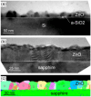
Development of crystalline structures of ZnO after 200 ALD cycles. a,b) Cross‐sectional TEM images showcased for deposition on a‐SiO2 (a) and c‐Al2O3 (b) substrates. c) A crystal orientation map for ZnO/Al2O3. a–c) Reproduced with permission.[ 71 ] Copyright 2020, American Chemical Society.
Figure 9
Figure 9
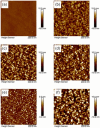
a–f) AFM images showing ALD ZrO2 films deposited at 150 °C (a) and 350 °C (b); deposited at 250 °C followed by annealing at 400 °C (c) and 1000 °C (d); and deposited at 250 °C with 200 cycles (e) and 800 cycles (f). Reproduced under the terms of the CC‐BY Creative Commons Attribution 4.0 International license (https://www.creativecommons.org/licenses/by/4.0).[ 72 ] Copyright 2019, The Authors, published by Springer Nature.
Figure 10
Figure 10
a–c) FE‐SEM images of ALD SnO2 nanowires with varying numbers of seed‐layer cycles, i.e., a) 215, b) 430, and c) 650, and d) their tunable aspect ratios. e,e′–g,g′) The effect of temperature is shown through FE‐SEM images and corresponding animated structure at 250 °C (e,e′), 300 °C (f,f′), and 350 °C (g,g′). a–g,g′) Reproduced with permission.[ 80 ] Copyright 2020, American Chemical Society.
Figure 11
Figure 11
Advanced ALD processes: a) discrete‐feeding ALD showing screening effect, b) a process recipe highlighting cut‐in purge steps, and c,d) a deposited DF‐ALD HfO2 film compared to typical ALD. a–d) Reproduced with permission.[ 82 ] Copyright 2023, Royal Society of Chemistry. e) An electric potential‐assisted ALD process chamber, f) comparison of surface area between nucleation stage and layer‐wise growth stage, and g–i) AFM images of control, positive bias, and negative bias for EA‐ALD Ru film at the nucleation stage. e–i) Reproduced with permission.[ 83 ] Copyright 2023, Royal Society of Chemistry.

References

    1. Seshan K., Schepis D., Handbook of Thin Film Deposition, William Andrew, Norwich, NY, USA: 2018.
    1. Baisnab D. K., Mukherjee S., Das S., in Chemical Solution Synthesis for Materials Design and Thin Film Device Applications (Eds: Das S., Dhara S.), Elsevier, Amsterdam, The Netherlands: 2021, pp. 231–275, 10.1016/B978-0-12-819718-9.00007-8. - DOI
    1. Putkonen M., Atomic Layer Deposition of Nanostructured Materials, John Wiley & Sons, Ltd., Hoboken, NJ, USA: 2011, pp. 41–59.
    1. Zaidi S. J. A., Basit M. A., Park T. J., Chem. Mater. 2022, 34, 7106.
    1. Short A., Jewell L., Bielecki A., Keiber T., Bridges F., Carter S., Alers G., J. Vac. Sci. Technol., A 2014, 32, 01A125.

LinkOut - more resources