. 2021 Jul 17;1(9):2100020.
doi: 10.1002/smsc.202100020. eCollection 2021 Sep.

Floating Interlayer and Surface Electrons in 2D Materials: Graphite, Electrides, and Electrenes

Affiliations

Floating Interlayer and Surface Electrons in 2D Materials: Graphite, Electrides, and Electrenes

Takeshi Inoshita et al. Small Sci. .

Abstract

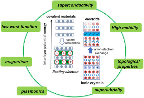
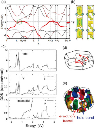
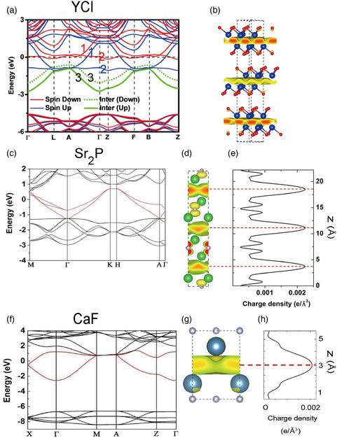
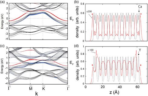
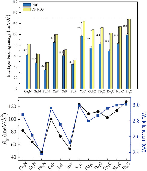
Over the last half century, layered materials have been at the forefront of materials science, spearheading the discovery of new phenomena and functionalities. Certain layered materials are known to possess electronic states unassociated with any of the constituent atoms, having a large proportion of their probability amplitude in the space between the layers. Usually, such a nucleus-free interlayer state has energy above the Fermi level and is unoccupied. However, the energy decreases when cations are intercalated and may cross the Fermi level, as in the case of C6Ca, a superconductor with a T c of 11.5 K. A major thrust to the research of interlayer electrons comes with the discovery of layered electrides, which are alternating stacks of positively charged ionic layers and negatively charged sheets of electrons in the interlayer space. When intercalation compounds and layered electrides are thinned down to the atomic scale, the interlayer states survive as surface states floating over the surface. This review provides a unified overview of the two classes of materials hosting interlayer floating electrons near the Fermi level, intercalation compounds and layered electrides, and their properties, including high electron mobility, low work function, ultralow interlayer friction, superconductivity, and plasmonic properties.

Keywords: 2D materials; electrides; graphite; layered materials; surface state; work functions.


Conflict of interest statement

The authors declare no conflict of interest.

Figures

Figure 1
Figure 1
Two types of layered material hosting interlayer states near the Fermi level.
Figure 2
Figure 2
Electronic structures of a–c) graphite and d–f) MLG calculated by DFT in the local density approximation. The ILBs in (a) are labeled IL1 and IL2. The signed PEDs (square of the wave function multiplied by its sign) for IL1 and IL2 at Γ are shown in (b,c), respectively. Although MLG has no interlayer space, it has surface states similar to the interlayer states of graphite. These so‐called “NFE” states are labeled NFE1 and NFE2 in (d). The signed PED for NFE1 and NFE2 at Γ are shown in (e,f), respectively. Courtesy of Dr. Masayuki Toyoda.
Figure 3
Figure 3
Band structures of a) C6Li, b) C3Li, c) C2Li, and d) C6Ca calculated using DFT. The ILBs are highlighted in red. The Fermi level is indicated by dashed lines. Adapted with permission.[ 11 ] Copyright 2005, Springer Nature.
Figure 4
Figure 4
a) Calculated energy band structure of bilayer graphene intercalated with Ca (C6CaC6). b) ARPES spectra of C6CaC6 and C6LiC6 at the Γ point. c,d) Band dispersion of C6CaC6 obtained by ARPES measurements along the high symmetry lines K′ΓK′ and M′ΓM′, respectively, showing ILBs (indicated as IL). Adapted with permission.[ 41 ] Copyright 2012, The National Academy of Sciences.
Figure 5
Figure 5
Electronic structure of an h‐BN monolayer under strain containing C impurities (donor) substituting B. The calculation was performed for a 4×4 supercell using DFT in the local‐density approximation. a) Band structure with/without strain. b) Electron density corresponding to the conduction band minimum at the Γ point under 5% compressive strain. Adapted with permission.[ 50 ] Copyright 2016, The American Physical Society.
Figure 6
Figure 6
a) Crystal structure of Ca2N. b–d) Electronic structure of Ca2N calculated using DFT. E F is set to zero. b) Energy band structure (left) and DOS (right). c) PED (left) and its isosurface (center) for the ILB (energy within 1.48 eV below E F), and electron localization function (right). d) Fermi surface. e,f) Measured electron transport properties of Ca2N: e) temperature dependence of resistivity (upper panel), electron concentration (middle panel), and Hall mobility (bottom panel) for both single‐crystal and polycrystal samples. f) Magnetoresistance measured at different temperatures for a single‐crystal sample. Adapted with permission.[ 27 ] Copyright 2013, Springer Nature.
Figure 7
Figure 7
Electronic structure of Y2C in the nonmagnetic phase calculated using DFT. a) Band structure, b) PED isosurface, c) DOS, d) Brillouin zone, and e) Fermi surface. The left (right) panel of (b) corresponds to electron energy −0.05 eV < EE F < 0.05 eV (−0.35 eV < EE F < −0.25 eV). The circle in (a) denotes the band crossing that renders the system a Dirac nodal‐line semimetal. The DOS in the bottom panel of (c) (indicated as “interstitial“) is obtained by placing an empty sphere of 1.8 Å radius at the interstitial sites (marked as X in Figure 6c) and projecting the wave functions onto this sphere. b) Reproduced under the terms of the CC‐BY 3.0 license.[ 28 ] Copyright 2014, The Authors, Published by The American Physical Society. c) Reproduced with permission.[ 59 ] Copyright 2015, The American Physical Society. e) Reproduced with permission.[ 58 ] Copyright 2014, The American Chemical Society.
Figure 8
Figure 8
a–c) Electronic structure of Y2C in the ferromagnetic phase calculated using DFT. a) Band structure, with the red and blue lines indicating the majority‐spin and minority‐spin bands, respectively. For comparison, the energy bands in the nonmagnetic phase are plotted by black dotted lines. b) Magnetization isosurface. c) Contour plot of magnetization in the ac plane indicated by V in (b). Reproduced with permission.[ 59 ] Copyright 2015, The American Physical Society. d) Squared magnetic form factor of Y2C derived from an inelastic neutron scattering measurement.[ 68 ] The orange line shows the squared form factor calculated from the magnetization density of a 4d electron in an yttrium atom. The latter cannot explain the measurement result. The dashed line is a guide for the eye. d) A modified version of Figure 3 in the previous study[ 68 ] provided by Dr. Hiromu Tamatsukuri.
Figure 9
Figure 9
a) Energy band structure of Gd2C calculated using DFT. The red and blue curves denote the majority‐spin and minority‐spin bands, respectively. The circles indicate band crossings that render the system a Weyl nodal‐line semimetal. Reproduced with permission.[ 123 ] Copyright 2020, The American Physical Society. b) Magnetization density of anionic electrons with energy within 0.1 eV below E F. Reproduced under the terms of the CC‐BY 3.0 license.[ 28 ] Copyright 2014, The Authors, Published by The American Physical Society.
Figure 10
Figure 10
a,b) Electronic structure of YCl in the ferromagnetic phase calculated using DFT. a) Band structure with the ILBs marked in green. b) The PED isosurface of the ILBs. a,b) Reproduced under the terms of the CC‐BY 4.0 license.[ 62 ] Copyright 2018, The Author, Published by Springer Nature. c–e) Electronic structure of Sr2P calculated using DFT. c) Electronic band structure. d) PED isosurface and e) plane‐averaged PED. f–h) Electronic structure of CaF calculated using DFT. f) Electronic band structure, g) PED isosurface, and h) plane‐averaged PED. The PED in (d,e) and (g,h) corresponds to the electron energy within 0.1 eV below E F. c–h) Reproduced with permission.[ 30 ] Copyright 2016, The American Chemical Society.
Figure 11
Figure 11
a) Energy band structure of a nine‐layer Ca2N slab calculated using DFT. The surface states are highlighted in red with the thickness proportional to the extra‐surface weight. b) Plane‐averaged PED (energy within 0.1 eV below E F) and total valence electron density, plotted as red solid and black dashed lines, respectively, for the same Ca2N slab. Each of the peaks marked by an asterisk in (b) corresponds to an extra‐surface floating state. c,d) Plots for Y2C corresponding to (a,b) are shown, respectively. Reproduced with permission.[ 79 ] Copyright 2017, The American Physical Society.
Figure 12
Figure 12
Interlayer binding energies E B of Q2DEs calculated using DFT. In the upper panel, the yellow and blue bars show the results obtained with and without considering van der Waals corrections (DFT‐D3) to the potentials. Reproduced with permission.[ 80 ] Copyright 2019, The American Chemical Society.
Figure 13
Figure 13
Electronic structure of Ca2N monolayer (electrene) calculated using DFT. a) Band structure with the lowest surface band highlighted in red. The black curve immediately above denotes the second surface band. These are the bonding and antibonding combinations of the floating electron states on the two sides of the layer, respectively. b) PED map of the lowest surface band at the Γ point. c) ELF. Reproduced with permission.[ 82 ] Copyright 2014, The American Chemical Society.
Figure 14
Figure 14
Work functions of Q2DEs calculated using DFT. Reproduced with permission.[ 30 ] Copyright 2016, The American Chemical Society.
Figure 15
Figure 15
a) Local DOS for MoTe2/Ca2N calculated using DFT before (upper panel) and after (lower panel) the two materials are brought into contact. In the 2D plots on the right, the horizontal and vertical axes correspond to energy and position z, respectively, and the DOS is shown by color. Note that the contact lifts the Fermi level of MoTe2 to about 0.15 eV above the conduction band bottom. Reproduced with permission.[ 89 ] Copyright 2017, The American Chemical Society. b–f) Electronic structure of a six‐layer slab of Ca2N with MLG placed on top. b,c) Layer‐averaged PED in the energy range −0.1 eV < EE F < 0 for Ca2N and MLG/Ca2N, respectively. The positions of the surface Ca layers are indicated at the top of (b). Note that the extra‐surface floating electrons (indicated by *) of Ca2N transfer almost entirely to the π orbitals of MLG upon contact. d,e) Color maps corresponding to (b,c), respectively. f) DOS of MLG in contact with Ca2N. The Fermi level of free‐standing MLG (E F0) is lifted into the π* band and pinned at the vHS, where DOS diverges logarithmically. Adapted with permission.[ 91 ] Copyright 2017, The American Physical Society.
Figure 16
Figure 16
a) Principal components of the dielectric tensor (permittivity) of Ca2N. The material is hyperbolic in the frequency region shown by the shaded area. b) EFCs given by Equation (1). The blue circle and red hyperbola show the EFC for vacuum and Ca2N, respectively. Here, k i ( k r) is the wave vector of the incident (refracted) wave, whereas S i and S r are the corresponding Poynting vectors. c) Schematic of negative refraction at a vacuum/Ca2N interface. The crystal c‐axis is parallel to the z‐direction. d) Simulation result of light propagation across vacuum/Ca2N interface. The color indicates the electric field strength, and the arrows show Poynting vectors. Reproduced with permission.[ 102 ] Copyright 2017, The American Physical Society.
Figure 17
Figure 17
a) Classification of topological semimetals. Reproduced with permission.[ 119 ] Copyright 2018, The Physical Society of Japan. b) Dirac nodal lines in the first Brillouin zone calculated for Y2C using DFT. Reproduced under the terms of the CC‐BY 4.0 license.[ 120 ] Copyright 2018, The Authors, Published by The American Physical Society. c) Weyl nodal lines in the first Brillouin zone calculated for ferromagnetic Gd2C using DFT. d) Fermi energy dependence of the anomalous Hall conductivity of Gd2C. c,d) Reproduced with permission.[ 123 ] Copyright 2020, The American Physical Society.
Figure 18
Figure 18
a) DOS calculated for (upper panel) Ca2N monolayer, (middle panel) semihydrogenated Ca2N monolayer, and (lower panel) fully hydrogenated Ca2N monolayer. b) Band structure of semihydrogenated Ca2N monolayer calculated using DFT with the PBE functional (black) and HSE functional (red). a,b) Reproduced with permission.[ 125 ] Copyright 2019, The American Chemical Society. c) Total and PDOS calculated for Ca2N monolayer after Na absorption. d) PED isosurface for Na‐absorbed Ca2N monolayer calculated for an energy window of −0.05 eV < EE F < 0.05 eV. c,d) Reproduced with permission.[ 126 ] Copyright 2015, The American Chemical Society.
Figure 19
Figure 19
Evolution of the crystal structure and ELF of Ca2N calculated using DFT under increasingly strong hydrostatic pressure. The space groups are a) R3¯m, b) Fd3¯m, c) I4¯2d, and d) Cc. Reproduced under the terms of the CC‐BY 4.0 license.[ 132 ] Copyright 2018, The Authors, published by Wiley‐VCH.

References

    1. Posternak M., Baldereschi A., Freeman A. J., Wimmer E., Weinert M., Phys. Rev. Lett. 1983, 50, 761.
    1. Ohno T., Nakao K., Kamimura H., J. Phys. Soc. Jpn. 1979, 47, 1125.
    1. Kamimura H., Nakao K., Ohno T., Inoshita T., Phys. B+C 1980, 99, 401.
    1. Catellani A., Posternak M., Baldereschi A., Jansen H. J. F., Freeman A. J., Phys. Rev. B 1985, 32, 6997. - PubMed
    1. Koma A., Miki K., Suematsu H., Ohno T., Kamimura H., Phys. Rev. B 1986, 34, 2434. - PubMed

LinkOut - more resources